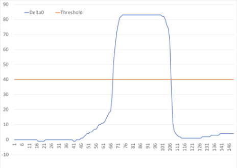
The simplest implementation of a capacitive sensor is a button, where the sensor consists of a single X-Y node and is interpreted as a binary state: In Detect or Out of Detect. When the touch delta – the digitized measurement of touch capacitance Ct – exceeds the touch threshold, the senor is In Detect.
Electrode Shapes
A sensor node is formed everywhere a pair of X and Y electrodes form an area of coupling. Common button shapes are round or rectangular, although any shape with parallel segment coupling of X and Y electrodes may be used.
Interleaved Key
The simplest sensor layout is a coplanar interleaved key. See Figure 2.
An interleaved key is typically between 8-20 mm wide. To avoid excess X-Y capacitance – and associated increase acquisition time – the electrode spacing must be increased for larger keys.
The electrode segment width must usually be the minimum track width available but may be increased up to 1 mm where the sensors are formed on a high-sheet resistance material such as ITO.
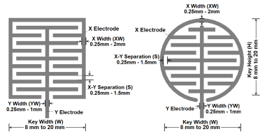
| Min. | Typical | Max. | |
|---|---|---|---|
| Key Height (H) | 8 mm | 12 mm | 20 mm |
| Key Width (W) | 8 mm | 12 mm | 20 mm |
| X Width (XW) | 0.25 mm | 0.5 mm | 2 mm |
| Y Width (YW) | 0.25 mm | 0.5 mm | 1 mm |
| X-Y Separation (S) | 0.25 mm | 0.5 mm | 1.5 mm |
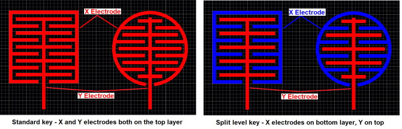
The interleaved key is typically implemented on a single PCB layer but may be split between two layers with the X electrodes on the layer furthest from the touch surface. A two-layer design combines high sensitivity with low default sensor capacitance. It provides a maximum length of the parallel segments under the touch contact for increased sensitivity while increasing X-Y separation and thus reducing the default sensor capacitance.
A two-layer interleaved sensor is highly suitable for implementation on a flex-PCB as it simplifies the routing for X and Y electrodes. However, with a thicker substrate, e.g, 1.6 mm FR4, a reduction in sensitivity may be expected.
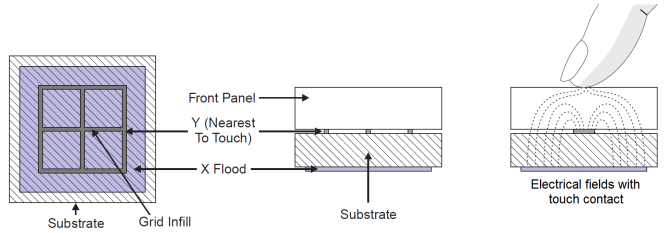
Flooded X Sensor
An alternative layout is ‘flooded X’, where the X electrode is implemented as a solid area behind a segmented Y electrode. The X area must extend beyond the Y electrode by at least 2 mm on each side.
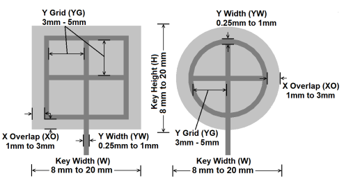
| Min. | Typical | Max. | |
|---|---|---|---|
| Key Height (H) | 8 mm | 12 mm | 20 mm |
| Key Width (W) | 8 mm | 12 mm | 20 mm |
| X Overlap (XO) | 1 mm | 2 mm | 3 mm |
| Y Width (YW) | 0.25 mm | 0.5 mm | 1 mm |
| Y Grid (YG) | 3 mm | 4 mm | 5 mm |
This layout also has the advantage that the X area shields the Y sensor from circuit noise from behind the X electrode. However, in an application requiring a thicker touch cover, flooded X sensors suffer from poor sensitivity.
Generally, flooded X sensors must only be used where the touch cover is thinner than the substrate separating the two electrodes. With standard 1.6 mm FR4 circuit boards, no touch cover thicker than 1.6 mm must be considered.