The project was developed using MPLAB X IDE and the peripherals required were configured using the MCC. The user can create a new project by clicking File → New Project → Standalone Project. The user must filter the devices and select the PIC16F18446, the microcontroller used in this application.
The purpose of this chapter is to familiarize users with the MPLAB Code Configurator and the structure of the generated code, and to demonstrate how to configure each of the peripherals used for developing this application.
- 1.Internal Oscillator
Figure 1. Internal Oscillator Configuration
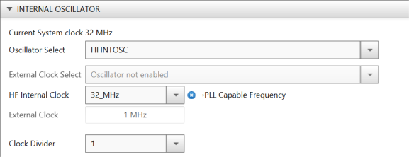
Internal Oscillator Configuration:
- Oscillator Select (NOSC): HFINTOSC
- Divider Selection (NDIV): 1
- Frequency Selection (HFFRQ): 32 MHz
- 2.ADCC
In this project, an analog potentiometer is used to adjust the oscillation frequency of the metronome. The variation of its resistance is transformed into a digital value by the ADCC. PIC18F18446 has an ADCC with a resolution of 12 bits, so the output of ADCC peripheral has a value between zero and 4095.
Because of the vulnerability of the mechanical parts of the potentiometer, its resistance value can be perturbed for short periods of time. To avoid this, the ADCC is configured in Average mode. It takes a series of samples and provides the average value as output. All the computation is done by hardware, with only the start of the conversions being triggered by the software.
Figure 2. ADCC Configuration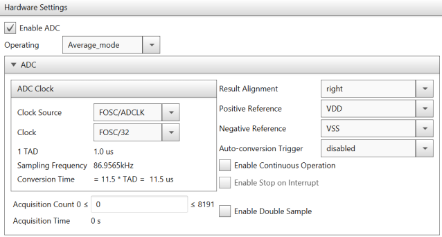
ADCC Configuration:
- ADCC Operating Mode (ADMD): Average mode
- ADCC Conversion Clock (ADCS): FOSC/32
- ADCC Results Alignment (ADFM): Right
- ADCC Positive Reference (ADNREF): VDD
- ADCC Negative Reference (ADPREF): VSS
- ADCC Enable (ADON): Check box
The settings regarding Average mode can be found by clicking the arrow near the ‘Computation Feature’ menu.
Figure 3. ADCC Computation Feature Menu Configuration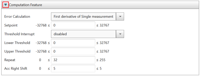
ADCC Computation Feature Menu Configuration:
- ADCC Error Calculation (ADCALC): First derivative of single measurement
- ADCC Threshold Interrupt (ADTMD): Disabled
- ADCC Repeat (ADRPT): 32
- ADCC Calculation Right Shift (ADCRS): 5
The number of samples that must be taken can be configured by writing the desired value in the Repeat box, or by configuring the ADRPT register.
When using the ADCC in Average mode, it is recommended that the number of samples be a power of two (ADRPT = 2ADCRS).
The ADCC can have various input channels, both internal and external. For this application, an external channel is used (ANA4) which utilizes PA4 pin. The signal that comes from the potentiometer is connected to this pin.
Figure 4. Pin Selection for ADCC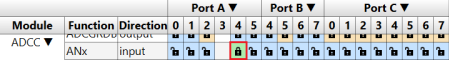
- 3.NCO
The NCO module is used to generate a square wave signal, which will be used as a clock signal for the rest of the peripherals, with the exception of the ADCC and CLC3. It repeatedly adds an increment value to an accumulator and each time the accumulator overflows, the output value toggles.
Figure 5. NCO Configuration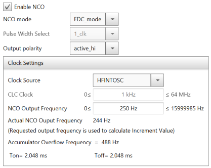
NCO Configuration:
- Pulse Frequency Mode (PFM): Fixed Duty Cycle mode
- Clock Source (CKS): HFINTOSC
- Polarity (POL): Active-high
- Enable (EN): Check box
The configuration has two modes of operation: Fixed Duty Cycle (FDC) mode and Pulse Frequency (PF) mode. In this project, the NCO module is configured in FDC mode, because the NCO_out is used as a clock signal.
The NCO_out frequency can be adjusted by writing the desired value to the NCO Output Frequency box or by configuring the NCO Increment (NCOxINC) register. The clock source for the NCO module is HFINTOSC, 32 MHz, because the application requires a fine frequency adjustment.
NCO_out is routed to a pin (PA2), in order to be available for all the peripherals.
Figure 6. Pin Selection for NCO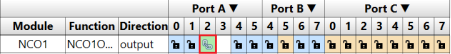
- 4.Timer0
Timer0 is used to divide the NCO_out frequency to obtain a signal whose value indicates the direction of movement for the metronome. There is a linear dependence between the number of steps run in a certain direction and the period of TMR0_out.
Figure 7. Timer0 Configuration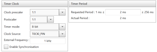 Timer0 Configuration:
- T0CKPS (Timer0 Prescaler Rate): 1:1
- T0OUTPS (Timer0 Output Postscaler): 1:1
- Timer mode: 8-bit mode
- T0CS (Timer0 Clock Source): T0CKI_PIN (pin selected by T0CKIPPS)
The Timer0 can run in two modes: the 8-bit mode and the 16-bit mode; this project uses the 8-bit mode.
The Timer0 period can be adjusted by writing the desired value to the Requested Period box or by configuring the Timer0 Period register (TMR0L, for 8-bit mode).
The clock source for Timer0 is NCO_out, but the two peripherals cannot be connected directly. The input clock source for Timer0 (T0CKI) is routed at the same pin as NCO_out (PA2). TMR0_out is routed to PB5 to be available for the CLC3.
Figure 8. Pin Selection for Timer0 Configuration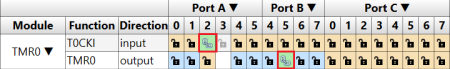
- 5.CLC1
The CLC1 is configured as a D-FF, with clock input represented by TMR2_out and with data (D) input represented by CLC1_out inverted. The S and R ports are not used and the OR gates from the CLC1 have the role of buffer and inverter.
Figure 9. Mode Selection for CLC1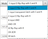
Mode selection for CLC1: 1-input D flip-flop with S and R.
Figure 10. CLC1 Configuration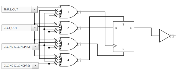
The CLC1_out drives Contact 1 and it is routed to two pins (PC0, PC1) configured as outputs, connected to the same contact. The two pins are used for the same contact in order to offer enough current for the motor.
Figure 11. Pin Selection for CLC1 Configuration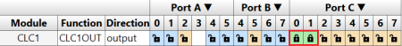
- 6.CLC2
The CLC2 is also configured as a D-FF, but it contains a multiplexer which selects the signal that will represent the data (D) input. The clock input is represented by the NCO_out and the R port is not used.
Figure 12. Mode Selection for CLC2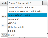
Mode selection for CLC2: 2-input D flip-flop with R.
Normally, a 2:1 multiplexer is formed from one inverter, one OR gate, and two AND gates, through the following configuration:
Figure 13. Typical 2:1 Multiplexer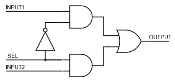
The output signal has the following expression:
However, the configuration of the CLC2 as D-FF does not contain AND gates. This inconvenient is solved by applying De Morgan’s Law on the relation mentioned above.
Figure 14. Multiplexer After Applying De Morgan’s Law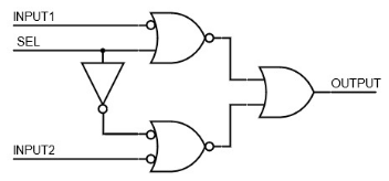
Each AND gate must be transformed into an NOR gate with its inputs inverted. After this operation, the output signal has the following expression:
The multiplexer from the CLC2 selects between the CLC1_out and CLC4_out, having the CLC3_out as the selection signal.
Figure 15. CLC2 Configuration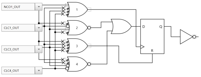
The CLC2_out is routed to four pins (PC2, PC3, PC4, PC5) configured as outputs and it drives the Contact 2 and Contact 3. The PC2 and PC3 are connected to one of the contacts, while PC4 and PC5 are connected to the other contact. Two pins are used for the same contact in order to offer enough current to the motor.
Figure 16. Pin Selection for CLC2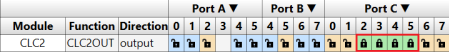
- 7.CLC4
The CLC4 is also configured as a D-FF, with a multiplexer that selects the signal that will represent the data (D) input. The clock input is represented by the NCO_out and the R port is not used.
Figure 17. Mode Selection for CLC4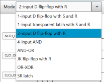
Mode selection for CLC4: 2-input D flip-flop with R.
Figure 18. Configuration for CLC4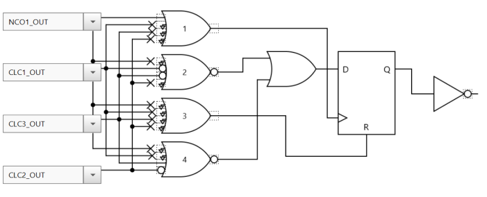
The multiplexer from CLC4 is implemented similarly as to the one from CLC2. It selects between CLC1_out and CLC2_out, and has the CLC3_out as selection signal.
The CLC4_out drives Contact 4 and it is routed to two pins (PC6, PC7) configured as outputs connected to the same contact. Two pins are used for the same contact in order to offer enough current to the motor.
Figure 19. Pin Selection for CLC4
- 8.CLC3
The CLC3 is configured as a 2:1 multiplexer. However, for this configuration, the AND gates are available.
Figure 20. Mode Selection for CLC3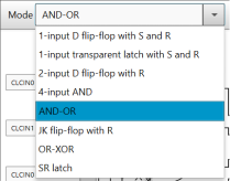
Mode selection for CLC3: AND-OR.
Figure 21. Configuration for CLC3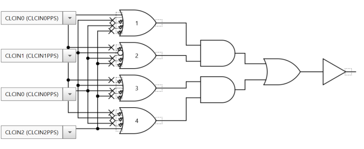
- 9.PPS
The TMR0_out, ‘Mode’, and ‘Direction’ signals cannot be routed directly to the CLC, so they are routed via the Peripheral Pin Select (PPS) module. The PPS allows the peripherals’ inputs and outputs to be rerouted to other I/O pins rather than to the default.
TMR0_out is routed to PB5 and the input signal CLCIN0 is routed to the same pin.
‘Mode’ signal is routed to PB4 and, in order to be accessible by CLC3, the CLCIN1 is also routed to PB4.
‘Direction’ signal is routed to PB6 and, in order to be accessible by CLC3, the CLCIN2 is also routed to PB6.
Figure 22. Pin Selection for CLC3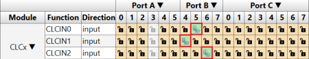
The audible signal is produced by a buzzer. In order to send a signal to it, an I/O pin (PA5) is configured as the output.
Figure 23. Pin Selection for Buzzer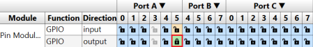
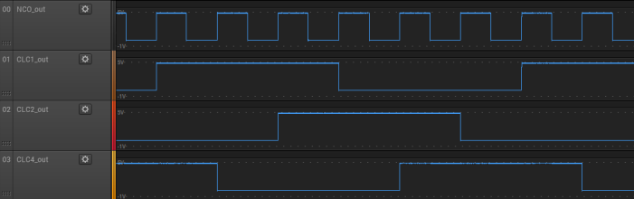
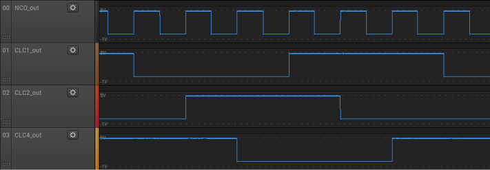
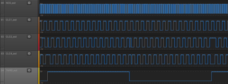
The following three images present the signals that drive the contacts of the motor (CLC1_out, CLC2_out, CLC4_out), the NCO_out, and TMR0_out for both clockwise and counterclockwise movements. There are the actual signals on the pins, captured by a logic analyzer.
The platform used is the PIC16F18446 Curiosity Nano with all the peripherals configured as described in the sections above.