The SAM-ICE JTAG connector is also compatible to ARM’s Serial Wire Debug (SWD).
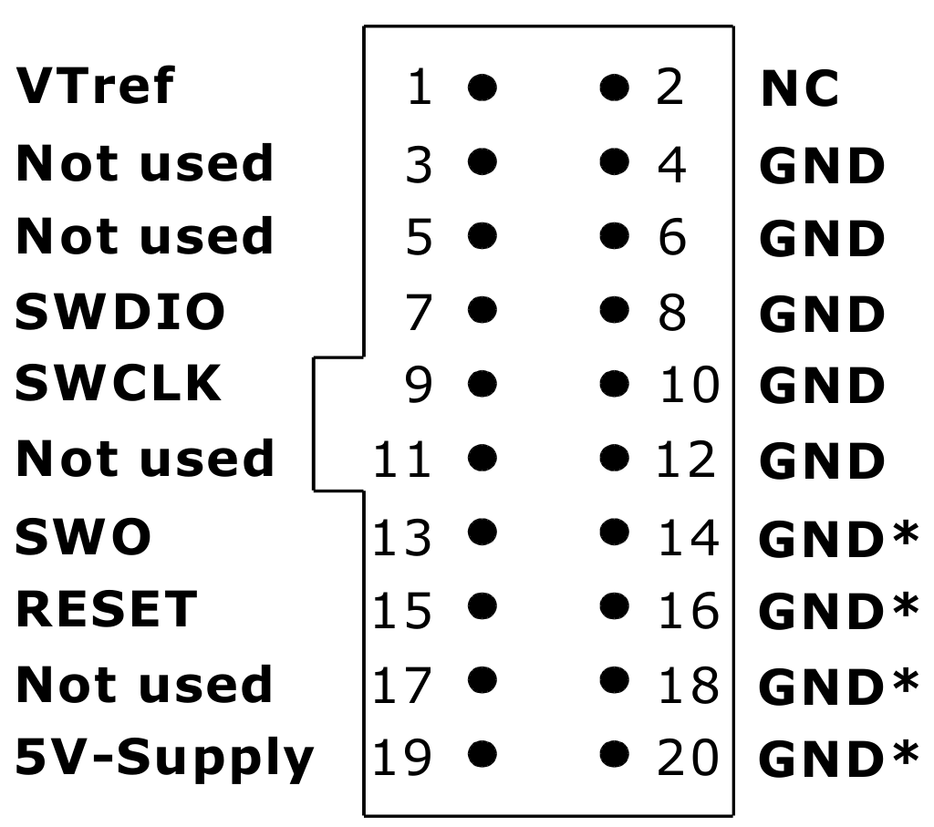
The table below lists the SAM-ICE SWD pinout.
| Pin | Signal | Type | Description |
|---|---|---|---|
| 1 | VTref | Input |
This is the target reference voltage. It is used to check if the target has power, to create the logic-level reference for the input comparators and controls the output logic levels to the target. It is normally fed from VDD on the target board and must not have a series resistor. |
| 2 | NC |
This pin is not connected |
|
| 3 | NC |
This pin is not used. If the device may also be accessed via JTAG, this pin may be connected to nTRST, otherwise leave open. |
|
| 4 | GND | Common ground | |
| 5 | NC |
This pin is not used. If the device may also be accessed via JTAG, this pin may be connected to TDI, otherwise leave open. |
|
| 6 | GND |
Common ground |
|
| 7 | SWDIO | Input/Output |
Single bi-directional data pin. A pull-up resistor is required. ARM recommends 100kΩ. |
| 8 | GND |
Common ground |
|
| 9 | SWCLK | Output |
Clock signal to target CPU. It is recommended that this pin is pulled to a defined state on the target board. Typically connected to TCK of target CPU. |
| 10 | GND |
Common ground |
|
| 11 | NC |
This pin is not used by the SAM-ICE when operating in SWD mode. If the device may also be accessed via JTAG, this pin may be connected to RTCK, otherwise leave open. |
|
| 12 | GND |
Common ground |
|
| 13 | SWO | Input |
Serial Wire Output trace port. (Optional, not required for SWD communication.) |
| 14 | GND |
Common ground |
|
| 15 | RESET | Input/Output |
Target CPU reset signal. Typically connected to the RESET pin of the target CPU, which is typically called "nRST", "nRESET", or "RESET". |
| 16 | GND |
Common ground |
|
| 17 | NC |
This pin is not connected in SAM-ICE |
|
| 18 | GND |
Common ground |
|
| 19 | NC |
This pin is not connected in SAM-ICE |
|
| 20 | GND |
Common ground |