The device used to develop the application described in this document is AVR128DA48. It is equipped with a 12-bit resolution ADC module that provides both Single-Ended and Differential modes.
The ADC input signal is fed through a Sample-and-Hold circuit which ensures that the input voltage to the ADC is held at a constant level during sampling. The ADC voltage reference is configured in the VREF peripheral.
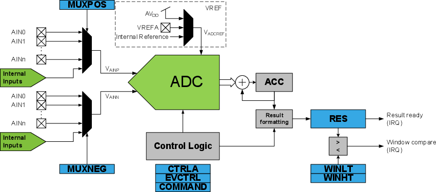
The block diagram of the ADC module is presented below.
To configure a module, the respective module registers must be used. The Register Summary and Register Description data sheet chapters provide a list of all registers of a module and describe the functionality of all the bits and bit fields of the module registers.
In this application example, the ADC will be configured in Differential mode. A differential ADC measures the voltage difference between two inputs. This can be essential in certain applications as some measurement concepts require two output signals, instead of one, to quantify the physical property of interest. Sensors that implement such concepts typically provide their output value as the voltage difference between two signals, also known as a differential signal. Other sensors might provide a differential output for added robustness even though the measurement itself generates a single-ended signal.
When connecting a differential analog sensor to an MCU, one of the signals in the differential pair is defined as the positive input, while the other is defined as the negative input. The value of the differential signal is the voltage of the positive input referenced to the negative input. The positive and negative designation of each signal determines the polarity of the differential signal, defining it as positive when the positive input is larger than the negative input, and negative if the negative input is larger than the positive input. The conversion result is given by the following equation:
Where VAINP and VAINN are the positive and negative ADC inputs, and VREF is the selected ADC voltage reference. The data format for differential conversions is two’s complement with sign extension.