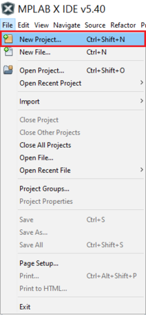
Follow these steps to generate the project using MCC:
- 1.Create a new MPLAB X project for AVR128DA48.
- 1.1.Open MPLAB X IDE v
5.40. Go to File>New Project.Figure 1. Create New Project
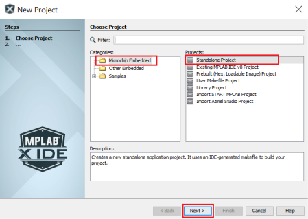
- 1.2.From the window that appeared
on the screen, select Microchip Embedded, followed by Standalone
Project, and then click Next. Figure 2. New Project – Choose Project
- 1.3.Select AVR128DA48 from
the Device tab and the AVR128DA48 Curiosity Nano (click
SN) from the Tool tab. Click Next.Figure 3. New Project – Select Device

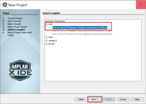
- 1.4.Select XC8 (v2.20)
Compiler and click Next.Figure 4. New Project – Select Compiler
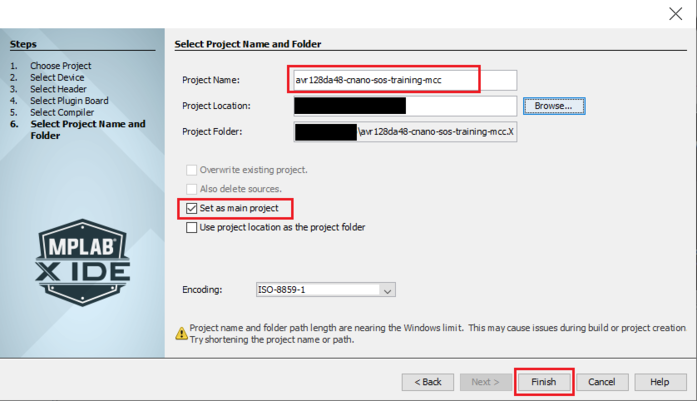
- 1.5.Insert a name for the project
and select the location where to be saved. Make sure that Set as main
project is checked and click Finish.Figure 5. New Project – Select Project Name and Folder
- 1.1.Open MPLAB X IDE v
5.40. Go to File>New Project.
- 2.Open the MCC from the
toolbar.
If the MCC is not installed, please follow the instructions provided on the MPLAB®InstallCode Configurator (MCC) webpage.
Figure 6. MCC Icon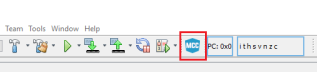
- 3.Add the peripherals and configure
them:
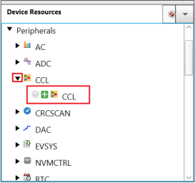
- 3.1.From the Device Resources
window, add CCL, EVSYS, TCA0, TCA1, and
TCD0. Select the peripheral to be added and click on the
‘+’ icon. Note: The image shows how to only add the CCL peripheral. Do the same operation for all the peripherals mentioned above.Figure 7. Add Peripherals
 The added peripherals can be found in Project Resources>Peripherals.Figure 8. Added Peripherals
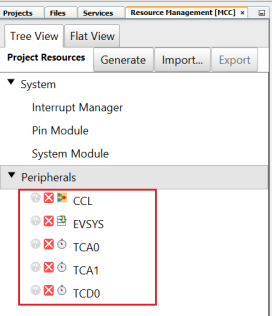
- 3.2.Perform the following configuration for each peripheral:
- TCD0
Configuration:
- Easy
Setup>Hardware Settings:Figure 9. TCD0-Easy Setup
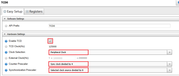
- Enable TCD check box: checked
- Clock Selection: Peripheral Clock
- Counter Prescaler: Sync clock divided by 4
- Synchronization Prescaler: Selected Clock Source divided by 8
After the configurations made above, the TCD0 clock will have a frequency of 125 kHz.
Note: The application is using the default clock configuration (Internal High Frequency Oscillator at 4 MHz). - Registers
tab:Figure 10. TDC0-Registers-CMPBCLR and CMPBSET
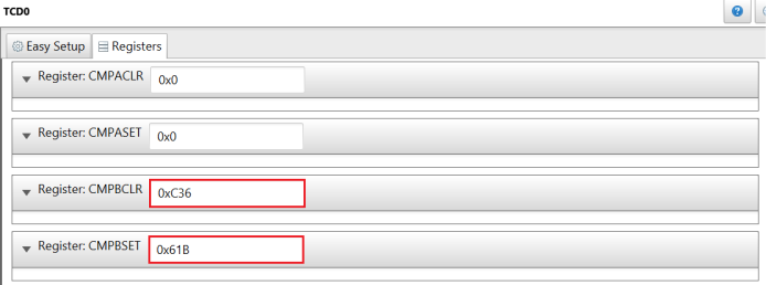
- Compare B Clear: 0xC36
- Compare B Set: 0x61B
The TCD0 will be configured to generate an event every time the counter reaches the value from CMPBSET register. The time difference between two consecutive events is TCD0 clock/CMPBCLR.
Because the events must occur with a frequency of 40 Hz, results that CMPBCLR = TCD0 clock/40 Hz = 0xC36.
Figure 11. TDC0-Registers-CMPB and CMPBEN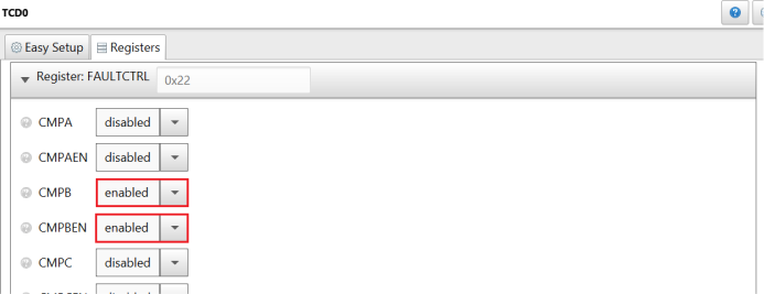
- Compare B Value: enabled
- Compare B Enable: enabled
After the configurations made above TCD will generate an event every 25 ms. This event will be later connected on this demo with the LUT0, TCA0 and TCA1.
- Easy
Setup>Hardware Settings:
- TCA0
Configuration:
- Easy
Setup>Hardware Settings:Figure 12. TCA0-Easy Setup-Hardware Settings
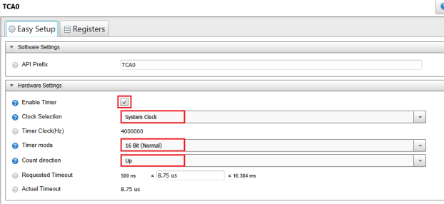
- Enable Timer check box: checked
- Clock Selection: System Clock
- Timer mode: 16 Bit (Normal)
- Count direction: Up
- Registers
tab:Figure 13. TCA0-Registers-PER
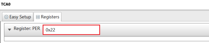
- Period: 0x22
In decimal 0x22=34, which is the number of dots from a SOS message period. In this way the TCA0 output will have a resolution of 1 dot.
- Easy
Setup>Waveform Generation Settings:Figure 14. TCA0-Easy Setup-Waveform Generation Settings
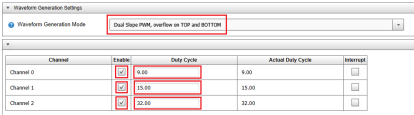
- Waveform Generation mode: Dual Slope PWM, overflow on TOP and BOTTOM
- Enable check box right next to Channel 0: checked
- Duty Cycle right next to Channel 0: 9.00
- Enable check box right next to Channel 1: checked
- Duty Cycle right next to Channel 1: 15.00
- Enable check box right next to Channel 2: checked
- Duty Cycle right next to Channel 2: 32.00
- Registers
tab:Figure 15. TCA0-Registers-CTRLC
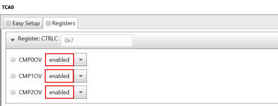
- Compare Output Value 0: enabled
- Compare Output Value 1: enabled
- Compare Output Value 1: enabled
Figure 16. TCA0-Registers-EVCTRL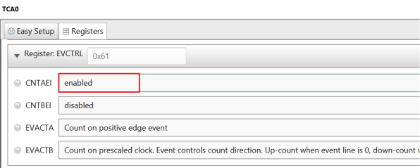
- Enable Counter Event Input A: enabled
TCA0 will count every time an event from TCD0 occurs.
- Easy
Setup>Hardware Settings:
- TCA1
Configuration:
- Easy
Setup>Hardware Settings:Figure 17. TCA1-Easy Setup-Hardware Settings
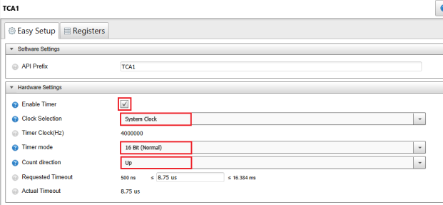
- Enable Timer check box: checked
- Clock Selection: System Clock
- Timer mode: 16 Bit (Normal)
- Count direction: Up
- Registers
tab: Figure 18. TCA1-Registers-PER
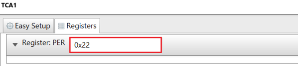
- Period: 0x22
In decimal 0x22=34, which is the number of dots from a SOS message period. In this way the TCA1 output will have a resolution of 1 dot.
- Easy
Setup>Waveform Generation Settings:Figure 19. TCA1-Easy Setup-Waveform Generation Settings
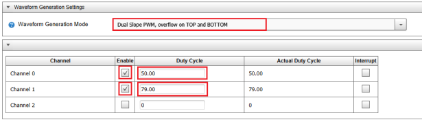
- Waveform Generation mode: Dual Slope PWM, overflow on TOP and BOTTOM
- Enable check box right next to Channel 0: checked
- Duty Cycle right next to Channel 0: 50.00
- Enable check box right next to Channel 1: checked
- Duty Cycle right next to Channel 1: 79.00
- Registers
tab:Figure 20. TCA1-Registers-CTRLC
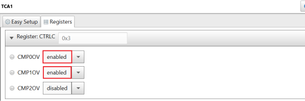
- Compare Output Value 0: enabled
- Compare Output Value 1: enabled
Figure 21. TCA1-Registers-EVCTRL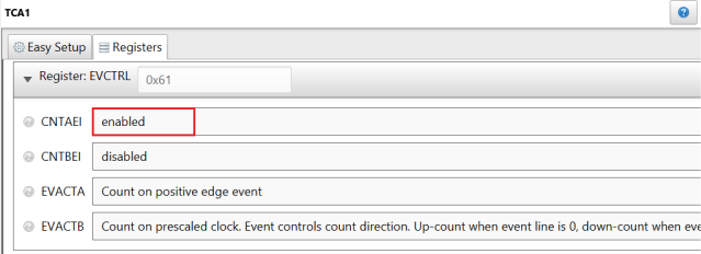
- Enable Counter Event Input A: enabled
TCA1 will count every time an event from TCD0 occurs.
- Easy
Setup>Hardware Settings:
- CCL
Configuration: The different instances of LUT can be selected from Easy Setup>CCL Settings. Click on the instance to be configured and make sure Enable CCL check box is checked.Figure 22. LUT Selection
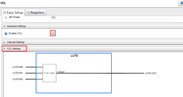
- Easy
Setup>CCL Settings:
- LUT0 Configuration: Figure 23. LUT0 Configuration
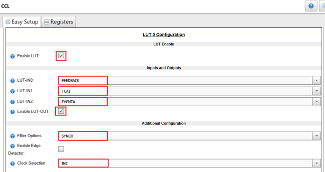
- Enable LUT check box: checked
- LUT-IN0: FEEDBACK
- LUT-IN1: TCA1
- LUT-IN2: EVENTA
- Enable LUT-OUT check box: checked
- Filter Options: SYNCH
- Clock Selection: IN2
The Filter from LUT0 is used in SYNC mode with feedback loop in order to obtain the signal which contains the pattern of letter ‘S’. It divides the frequency of events triggered by TCD0 with a factor of 4.
Figure 24. LUT0 Truth Table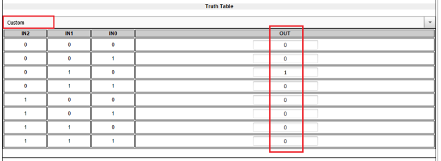
- Truth Table: Custom
- OUT: (from top to bottom) 00100000
- LUT1 Configuration:Figure 25. LUT1 Configuration
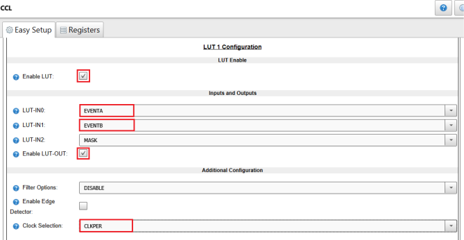
- Enable LUT check box: checked
- LUT-IN0: EVENTA
- LUT-IN1: EVENTB
- LUT-IN2: MASK
- Enable LUT-OUT check box: checked
- Filter Options: DISABLE
- Clock Selection: CLKPER
Figure 26. LUT1 Truth Table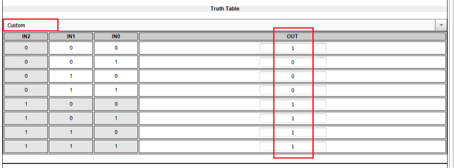
- Truth Table: Custom
- OUT: (from top to bottom) 10001111
The value of OUT bits is negated because the output of LUT1 will drive the CNANO board LED, which works on invert logic (logic ’0’ - ON, logic ‘1’ - OFF).
- LUT2 Configuration:Figure 27. LUT2 Configuration
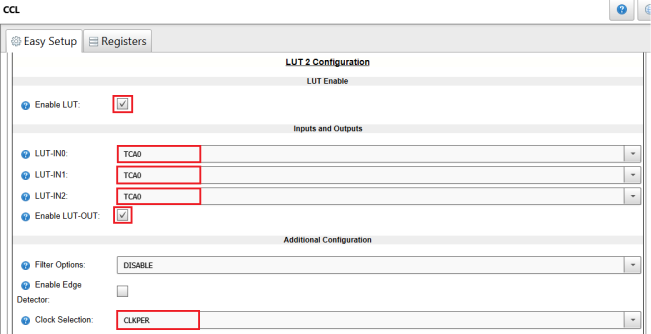
- Enable LUT check box: checked
- LUT-IN0: TCA0
- LUT-IN1: TCA0
- LUT-IN2: TCA0
- Enable LUT-OUT check box: checked
- Filter Options: DISABLE
- Clock Selection: CLKPER
Figure 28. LUT2 Truth Table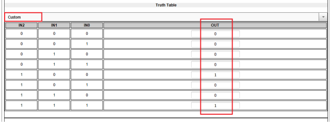
- Truth Table: Custom
- OUT: (from top to bottom) 00001001
- LUT3 Configuration:Figure 29. LUT3 Configuration
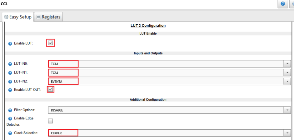
- Enable LUT check box: checked
- LUT-IN0: TCA1
- LUT-IN1: TCA1
- LUT-IN2: EVENTA
- Enable LUT-OUT check box: checked
- Filter Options: DISABLE
- Clock Selection: CLKPER
Figure 30. LUT3 Truth Table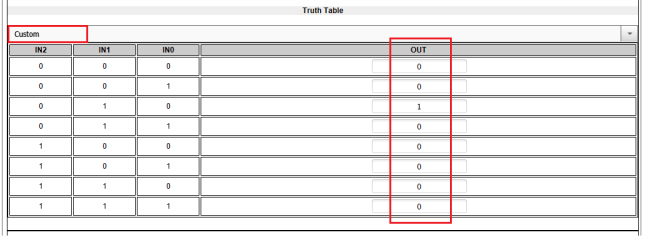
- Truth Table: Custom
- OUT: (from top to bottom) 00100000
- LUT0 Configuration:
- Easy
Setup>CCL Settings:
- EVSYS
Configuration:
- Event
Generators:
- CHANNEL0: TCD0_CMPBSET
- CHANNEL1: CCL_LUT0
- CHANNEL2: CCL_LUT3
- CHANNEL3: CCL_LUT2
Figure 31. EVSYS Event Generators
- Event
Users
- CHANNEL0: CCLLUT0A, TCA0CNTA, TCA1CNTA
- CHANNEL1: CCLLUT3A
- CHANNEL2: CCLLUT1A
- CHANNEL3: CCLLUT1B
Figure 32. EVSYS Event Users (1)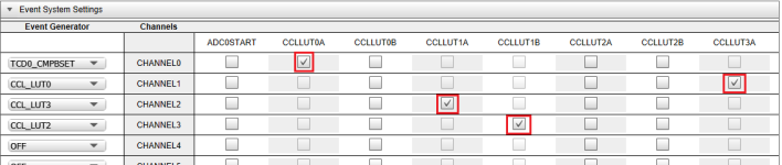 Figure 33. EVSYS Event Users (2)
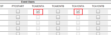
- Event
Generators:
- TCD0
Configuration:
- 3.1.From the Device Resources
window, add CCL, EVSYS, TCA0, TCA1, and
TCD0. Select the peripheral to be added and click on the
‘+’ icon.
- 4.Go to Pin Manager>Grid
View and perform the following configurations:
- Set Port A pin 3 (RA3) as output for LUT0
- Set Port C pin 6 (RC6) as output for LUT1
- Set Port D pin 3 (RD3) as output for LUT2
- Set Port F pin 3 (RF3) as output for LUT3
Figure 34. Pin Module CLC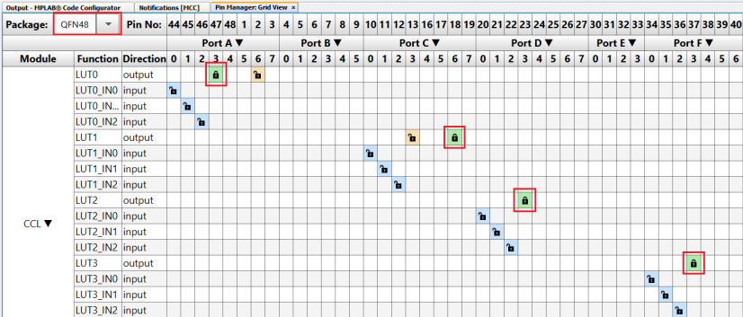
- Set Port A pins 0-2 (RA0-RA2) as output for TCA0
- Set Port B pins 0-2 (RB0-RB2) as output for TCA1
- Set Port A pins 4-7 (RA4-RA7) as output for TCD0
Figure 35. Pin Module Timers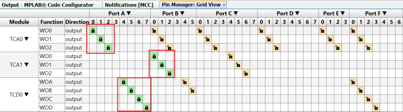 Note: The SOS signal will be available on the RC6. The rest of the signals have a correspondent output pin only for debugging.