The peripherals used for implementing this application are:
- Timer/Counter Type A (TCA)
- Timer/Counter Type D (TCD)
- Configurable Custom Logic (CCL)
- Event System (EVSYS)
The block diagram below presents the peripherals and connections between them. The red-marked lines represent event channels, while the blue-marked lines represent internal signals.
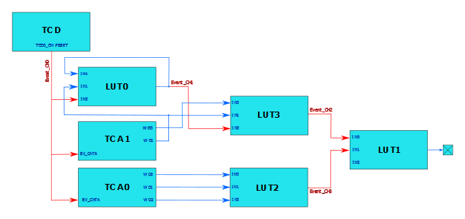
As mentioned in a section above, the reference clock must have a period of 25 ms (and a frequency of 40 Hz). It is generated using TCD0, which triggers events with that specific frequency. The event will be used as clock input for LUT0, TCA0, and TCA1.
TCA1 is used to generate M1 and M2 signals through TCA1-WO0 and TCA1-WO1 outputs, which will be connected to LUT0 and LUT3 as inputs.
TCA0 is used to generate M3, M4, and M5 signals through TCA0-WO2, TCA0-WO1, and TCA0-WO0 outputs, which will be connected to LUT2 as inputs.
LUT0 is used to generate the signal that contains the pattern for the letter ‘S’ (S’). The frequency of the S’ signal is double the frequency of the events that come from TCD0, because the Feedback feature was used.
LUT3 is used to perform the logic operation mentioned in Section 2.2.1 Generate the Waveform for the Letters ‘S’. Its output represents the SS signal and is connected with LUT1 through an event channel.
LUT2 is used to perform the logic operation mentioned in Section 2.2.2 Generate the Waveform for the Letter ‘O’. Its output represents the O signal and is connected with LUT1 through an event channel.
LUT1 is used to perform the logic operation mentioned in Section 2.2.3 Obtain the Waveform for the SOS Message and to output the SOS message on the CNANO board LED. Its inputs are represented by the events generated by LUT2 and LUT3.
The EVSYS is used to interconnect the peripherals.