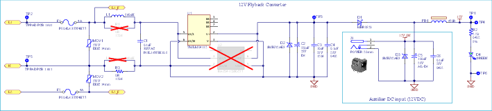
- An AC power source (mains grid) from 90 to 264 Vac and from 47 to 63 Hz, connected to the J1 and J2 connectors
- A +12V DC power source via a 2.1 mm center-positive plug into the power jack connector of the board (J3). The recommended rating capacity of the power adapter is 1.5A
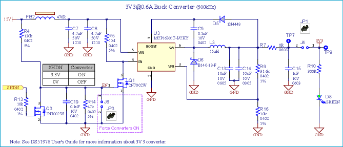
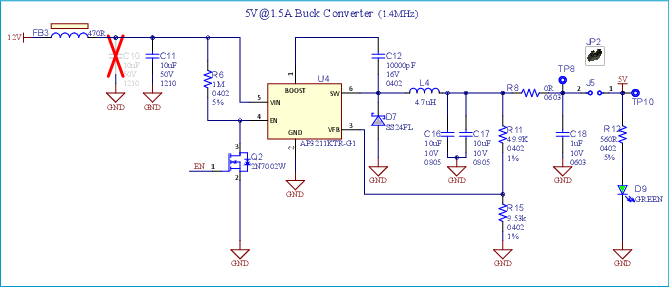
- +12V to power the 3.3V and 5V converters
- +3.3V to power the IC devices, such as PIC32CXMTSH, SST26VF016B and some interfaces
- +5V to power the mikroBUS and Xplained PRO connectors
The +5V voltage rail is obtained from the buck converter. Another LED, D9, and two test points, TP8 and TP10, are connected to the voltage rail to check whether power supply is connected. The jumper, J5, allows measuring the current on the 5V rail.
The processor manages the SHDN signal to shut down both buck converters and makes the processor enter Backup mode and the board enter a Power-Down mode. The SHDN signal controls the ENABLE signal of converters through a simple scheme with a FET (Field Effect Transistor). The SHDN signal can be disabled when the shunt JP3 is placed in J6; then, converters are always enabled. Note that using the SHDN pin when entering the backup mode is optional. See the Power Supply and Power Control section of the PIC32CXMTSH Data Sheet.
A 3V coin battery holder, BT1, is included to insert a CR2032 battery to supply VBAT voltage. It allows the microcontroller to be supplied even if a Brown-Out event occurs. The system is able to detect this event (see the Power Supply Monitor schematic below) and the embedded firmware may then switch to a Low-power mode to consume the lowest-possible amount of energy. While in Back-up mode, the board can be woken up by action on the SW2 button (Force Wake-Up) or SW3 button (Tamper), which signals the MCU to resume operations.
See the Power Supply and Power Control section of the PIC32CXMTSH Data Sheet for further descriptions about Backup mode and possible other wake-up sources.
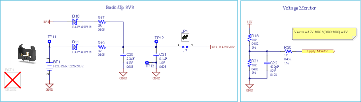
The jumper, J7, allows measuring the current on the back-up rail.