On the AVR DA devices, the Flash memory is mapped in the code space and it is
word-accessible through the LPM and SPM instructions.
Additionally, the Flash memory can be mapped in the CPU data space. This means that it
shares the same address space and instructions as SRAM, EEPROM, and I/O registers and is
accessible using the LD/ST instructions in assembly.
0x0000(PROGMEM_START) when accessed as program memory viaLPM/SPMinstructions;0x8000(MAPPED_PROGMEM_START) when accessed as data memory viaLD*/ST*instructions.
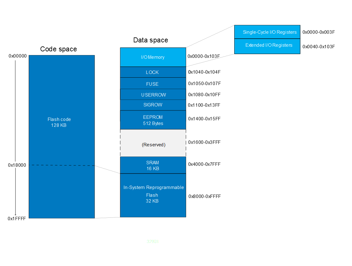
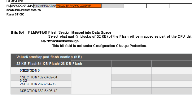
The size of the In-System Reprogrammable Flash in the data space is 32 KB. For devices with Flash memory size greater than 32 KB, the Flash memory is divided into blocks of 32 KB. Those blocks are mapped into the data space using the FLMAP bit field in the NVMCTRL.CTRLB register:
Another major difference between the tinyAVR®
and megaAVR® devices compared to the AVR DA devices is the
Flash write access. On the previous tinyAVR and megaAVR devices, the Flash writes are
performed through a page buffer, while on the AVR DA devices the writes are done
directly to Flash memory locations using ST/SPM
instructions.
0xFF),
otherwise the result will be an AND between the existing value and the
new one.