The ATA8510/15 consists of an analog front end, digital signal processing blocks (DSP), an 8-bit AVR sub-system and various supply modules such as oscillators and power regulators. A hardware block diagram of the ATA8510/15 shows in the following figure.
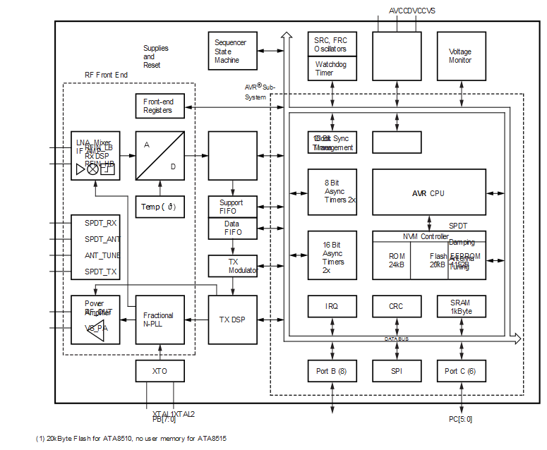
Together with the fractional-N PLL, the crystal oscillator (XTO) generates the local oscillator (LO) signal for the mixer in RXMode. The RF signal comes either from the Low-Band input (RFIN_LB) or from the High-Band input (RFIN_HB) and is amplified by the low-noise amplifier (LNA) and down-converted by the mixer to the intermediate frequency (IF) using the LO signal. A 10 dB IF amplifier with low-pass filter characteristic is used to achieve enhanced system sensitivity without affecting blocking performance.
After the mixer, the IF signal is sampled using a high-resolution analog-to-digital converter (ADC).
Within the RX digital signal processing (RX DSP), the received signal from the ADC is filtered by a digital channel filter and demodulated. Two data receive paths, path A and path B, are included in the RX DSP after the digital channel filter. In addition, the receive path can be configured to provide the digital output of an internal temperature sensor (Temp(ϑ)).
In TXMode, the fractional-N PLL generates the TX frequency. The power amplifier (PA) generates an RF output power signal programmable from -10 dBm to +14 dBm at RF_OUT. The FSK modulation is performed by changing the frequency setting of the fractional-N PLL dynamically with TX digital signal processing (TX DSP). Digital preemphasis and digital Gauss filtering can be activated in the TX DSP to achieve higher data rates or reduce occupied bandwidth. The ASK modulation is performed by switching the power amplifier on and off. An ASK shaping filter is available to reduce the transmitted bandwidth of the modulated PA output signal. The shaping filter can also be used at the start and end of an FSK transmission.
With the single pole double throw (SPDT) switch, the RF signal from the antenna is switched to RFIN in RXMode and from RF_OUT to the antenna in TXMode. An adjustable capacitor and an RF level detector on ANT_TUNE are used to tune the center frequency of loop antennas to reduce tolerances and capacitive proximity effects.
The system is controlled by an AVR CPU with 24 KB firmware ROM and 20 KB user Flash for the ATA8510. 1024-byte EEPROM, 1024-byte SRAM and other peripherals are supporting the transceiver handling. Two GPIO ports, PB[7:0] and PC[5:0], are available for external digital connections, for example, as an alternate function the SPI interface is connected to port B. The ATA8510/15 is controlled by the EEPROM configuration and SPI commands and the functional behavior is mainly determined by firmware in the ROM. Much of the configuration can be modified by the EEPROM settings. The firmware running on the AVR gives access to the hardware functionality of the ATA8510/15. Extensions to this firmware can be added in the 20 KB of Flash memory for the ATA8510. The RX DSP and TX DSP registers are addressed directly and accessible from the AVR. A set of sequencer state machines is included to perform RX and TX path operations (such as enable, disable, receive, transmit) which require a defined timing parallel to the AVR program execution.
The power management contains low-dropout (LDO) regulators and reset circuits for the supply voltages VS, AVCC, DVCC and VS_PA of the ATA8510/15. In OFFMode, all the supply voltages AVCC, DVCC and VS_PA (only use VS_PA for 2.5-5.5V operation) are switched off to achieve very low current consumption. The ATA8510/15 can be powered up by activating the PWRON pin or one of the NPWRON[6:1] pins because they are still active in OFFMode. The AVCC domain can be switched on and off independently from DVCC. The ATA8510/15 includes two idle modes. In IDLEMode(RC), only the DVCC voltage regulator, the FRC and SRC oscillators are active, and the AVR uses a power-down mode to achieve low current consumption. The same power-down mode can be used during the inactive phases of the PollingMode. In IDLEMode(XTO), the AVCC voltage domain as well as the XTO are additionally activated.
An integrated watchdog timer is available to restart the ATA8510/15 when it is not served within the configured time-out period.