The ADC can be used to convert both analog and digital signals. The signals may come from external sources via a port pin, or from internal sources. The ADC Positive Channel Selection (ADPCH) register controls the input multiplexer and determines which analog input channel is connected to the sampling circuit.
There may be several external input channels depending on the pin count of the selected device, but only one channel, either internal or external, can be selected and converted at a time. To determine the number and location of ADC channels in any PIC® device, refer to the specific device data sheet. Many data sheets list the location of each channel in the ‘Pin Diagrams’ charts. Each external channel is labeled ‘ANxy’, where ‘x’ refers to the I/O port, and ‘y’ refers to the pin within the port. For example, an external input signal, ANA1, points to the analog channel of PORTA, pin one.
Older data sheets, or data sheets for low pin count devices may label each external channel simply as ‘ANx’, where ‘x’ is the input channel number and may or may not refer to the actual port pin. For example, a 16-lead device may use the label AN1, but AN1 may point to PORTA’s pin number two.
When converting an analog input signal, the I/O pin must be configured as an input by setting the port pin’s TRIS bit corresponding to the selected input channel. Additionally, the pin must be configured as an analog input by setting the port pin’s ANSEL bit. It is important to note that analog voltages on any pin that is not defined as an analog input may cause the input buffer to conduct excess current.
When converting a digital signal, care must be taken when considering the ANSEL selection. If the ADC is to convert a digital input signal, the port pin’s ANSEL bit should be cleared. The ADC can also read and convert a digital output signal. In this case, the ANSEL bit can be cleared.
When switching between input channels, an acquisition delay is required before starting the next conversion. The acquisition delay is required to meet the ADC’s specified accuracy. The delay allows time for the sampling capacitor to fully charge to the input voltage level.
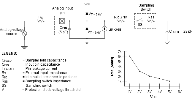
External source impedance (RS), internal interconnect impedance (RIC), and sampling switch impedance (RSS) have a direct effect on the acquisition time (see figure below). Microchip typically recommends a maximum source impedance of no greater than 10 kΩ. The device-specific recommended maximum source impedance can be found in the device data sheet’s electrical specifications. Higher impedance values require a longer acquisition time, and, as impedance is decreased, acquisition time may be decreased.
Refer to Figure 2 to calculate the minimum acquisition time. This equation assumes that the sample and hold capacitor is charged to within one-half of a Least Significant bit (LSb), which is the maximum error allowed for the ADC to meet its specified resolution.
Where:
TAD = ADC example clock period (2 us)
TCOFF = Temperature Coefficient = (Temperature - 25°C) *
TC = Hold Capacitor Charging Time =
Where:
CHOLD = sample and hold capacitor value (typical 28 pF)
RIC = internal interconnect impedance (1 kΩ typical)
RSS = internal sampling switch impedance (varies depending on VDD, see Figure 1)
RS = external analog source impedance
Example:
Find TACQ(MIN) when the temperature is 30°C, VDD = 5V, ADC resolution = 12 bits, and input impedance is 1 kΩ:
First, TC is unknown, so it must be calculated:
Next, calculate TACQ:
Since the example ADC clock period is 2.0 us and the TACQ is 2.77 us, it will take two ADC clock periods to complete the conversion. The ADC Acquisition Time Control Register pair (ADACQH:ADACQL) can now be loaded with the register value corresponding to two ADC clock periods.