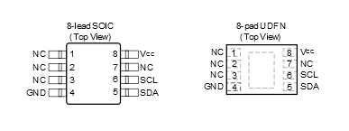
| Pin | Function I2C Devices |
|---|---|
| NC | No Connect |
| GND | Ground |
| SDA | I2C Serial Data |
| SCL | I2C Serial Clock Input |
| VCC | Power Supply |
Figure 1. UDFN and SOIC Pinout
Note: It is recommended that the UDFN backside
paddle be connected to GND.
| Pin | Function I2C Devices |
|---|---|
| NC | No Connect |
| GND | Ground |
| SDA | I2C Serial Data |
| SCL | I2C Serial Clock Input |
| VCC | Power Supply |