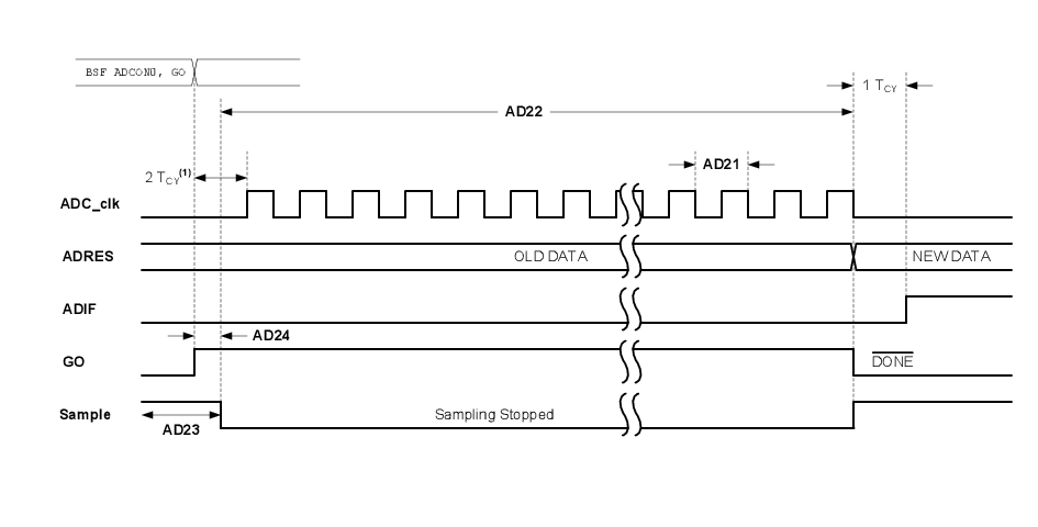
| Standard Operating Conditions (unless otherwise stated) | |||||||
|---|---|---|---|---|---|---|---|
| Param No. | Sym. | Characteristic | Min. | Typ. † | Max. | Units | Conditions |
| AD20 | TAD | ADC Clock Period | 0.5 | — | 9 | μs | FOSC clock source |
| AD21 | 1 | 2 | 6 | μs | ADCRC clock source | ||
| AD22 | TCNV | Conversion Time | — | 11 | — | TAD | Set of GO bit to clear of GO bit |
| AD23 | TACQ | Acquisition Time | — | 2 | — | μs | |
| AD24 | THCD | Sample and Hold Capacitor Disconnect Time | — | — | — | — | FOSC clock source |
|
* - These parameters are characterized but not tested. † Data in “Typ” column is at 3.0V, 25°C unless otherwise stated. These parameters are for design guidance only and are not tested. |
|||||||
Figure 1. ADC Conversion Timing (ADC Clock
FOSC-Based)
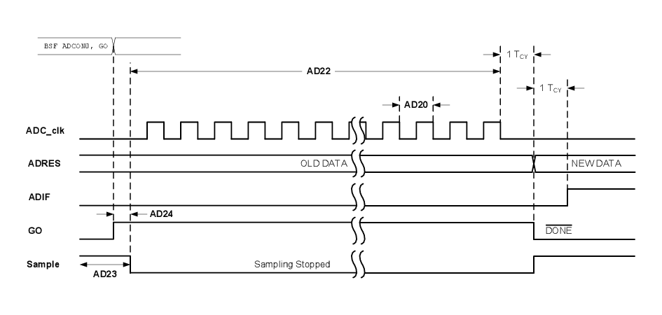
Figure 2. ADC Conversion Timing (ADC Clock
from ADCRC)
Note:
- 1.If the ADC clock source is
selected as ADCRC, a time of TCY is added before the ADC clock
starts. This allows the
SLEEPinstruction to be executed.