The strength of the crystal driver circuit determines the characteristics of the sine wave output of the crystal oscillator. The sine wave is the direct input into the digital clock input pin of the microcontroller. This sine wave must easily span the input minimum and maximum voltage levels of the crystal driver’s input pin while not being clipped, flattened or distorted at the peaks. A too low sine wave amplitude shows that the crystal circuit load is too heavy for the driver, leading to potential oscillation failure or misread frequency input. Too high amplitude means that the loop gain is too high and may lead to the crystal jumping to a higher harmonic level or permanent damage to the crystal.
Determine the crystal's output characteristics by analyzing the XTAL1/TOSC1 pin voltage. Be aware that a probe connected to the XTAL1/TOSC1 leads to added parasitic capacitance, which must be accounted for.
The loop gain is negatively affected by temperature and positively by voltage (VDD). That means that the drive characteristics must be measured at the highest temperature and lowest VDD, and the lowest temperature and highest VDD at which the application is specified to operate.
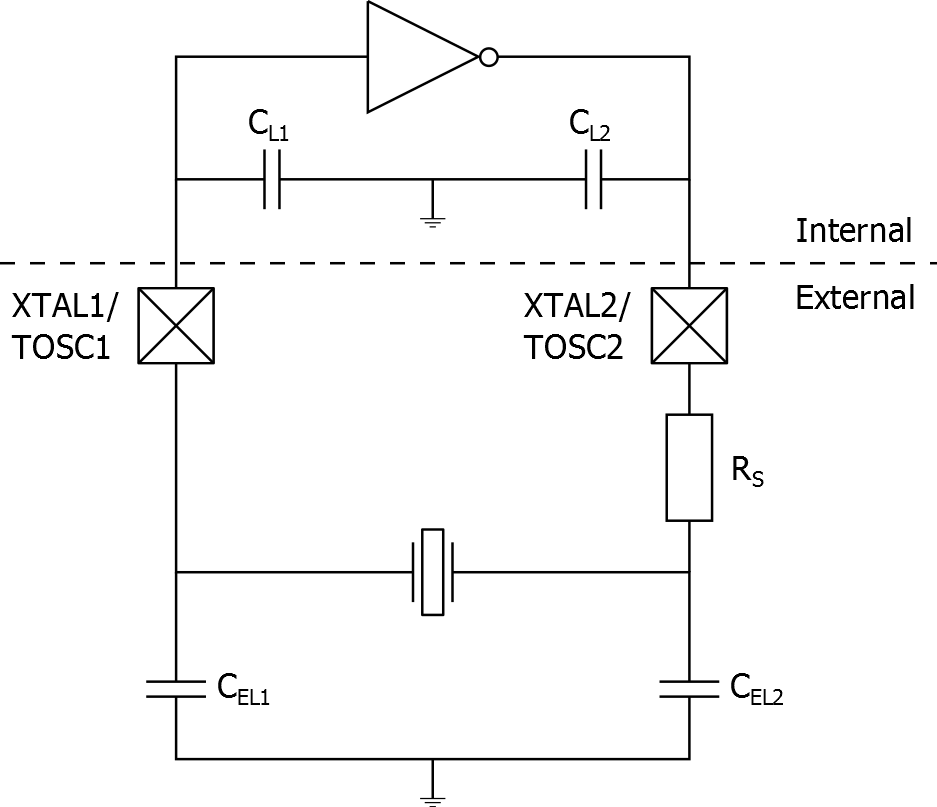
Select a crystal with lower ESR or capacitive load if the loop gain is too low. If the loop gain is too high, a series resistor, RS, may be added to the circuit to attenuate the output signal. The figure below shows an example of a simplified crystal driver circuit with an added series resistor (RS) at the output of the XTAL2/TOSC2 pin.