The simplest mode of using the ADC is to make a single conversion. The ADC
input pin needs to have the digital input buffer and the pull-up resistor disabled, in
order to have the highest possible input impedance. Pin PD6/AIN6 is used for ADC input
in this example.
Figure 1. ADC0.MUXPOS Selection
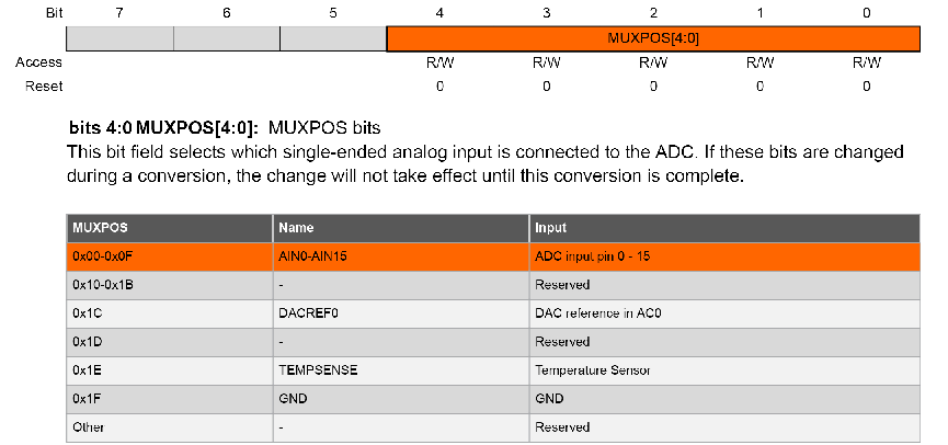
ADC0.MUXPOS = ADC_MUXPOS_AIN6_gc;
The ADC Clock Prescaler can be used to divide the clock frequency. In this
particular example, the clock is divided by 4. The ADC can use VDD, external
reference or internal reference for its positive reference. The internal reference is
used in this example.
Figure 2. ADC0.CTRLC Voltage Reference
Selection
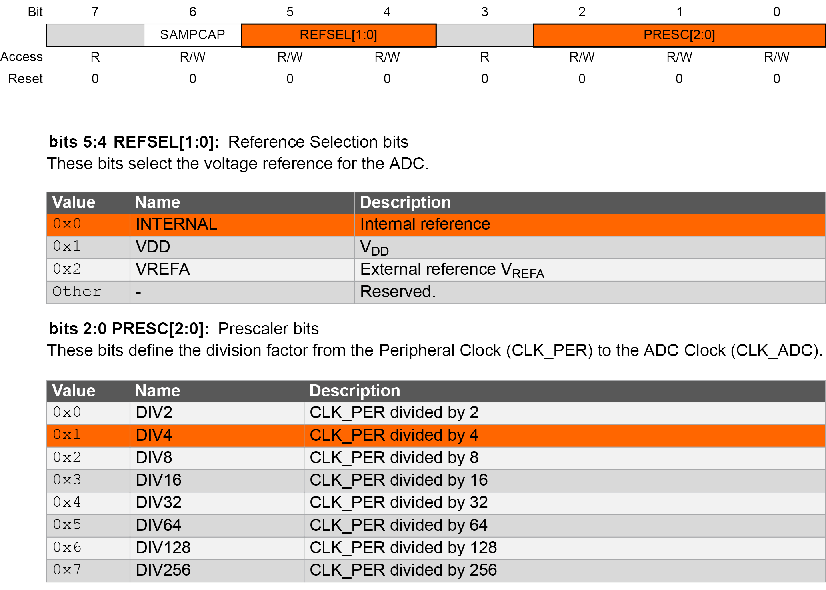
ADC0.CTRLC |= ADC_PRESC_DIV4_gc;
ADC0.CTRLC |= ADC_REFSEL_INTREF_gc;
The ADC resolution is set by the RESSEL bit in the ADC0.CTRLA register. The
ADC is enabled by setting the ENABLE bit in the ADC0.CTRLA register.
Figure 3. ADC0.CTRLA Resolution
Selection
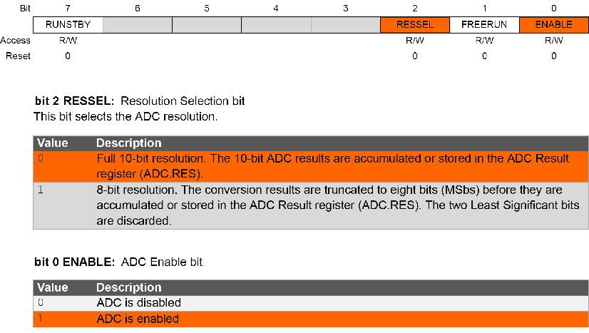
ADC0.CTRLA |= ADC_RESSEL_10BIT_gc;
ADC0.CTRLA |= ADC_ENABLE_bm;
The ADC conversion is started by setting the STCONV bit in the ADC0.COMMAND
register.
Figure 4. ADC0.COMMAND - Start
conversion
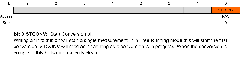
ADC0.COMMAND = ADC_STCONV_bm;
When the conversion is done, the RESRDY bit in the ADC0.INTFLAGS gets set by
the hardware. The user must wait for that bit to get set before reading the ADC
result.
Figure 5. ADC0.INTFLAGS - hardware-set
RESRDY bit
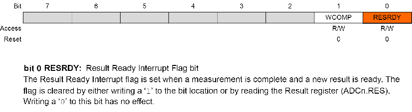
while (!(ADC0.INTFLAGS & ADC_RESRDY_bm))
{
    ;
}
The user must clear the RESRDY bit by writing ‘
1’ to it
before starting another
conversion.ADC0.INTFLAGS = ADC_RESRDY_bm;
The conversion result can be read from the ADC0.RES
register.
adcVal = ADC0.RES;

Tip: The full code example is also
available in the Appendix section.