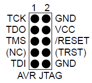
When designing an application PCB, which includes an AVR with the JTAG interface, it is recommended to use the pinout as shown in the figure below.
For other AVR connections, see AT Devices - On-Chip Debugging (OCD).
Figure 1. AVR JTAG Header Pinout
| Name | Pin | Description |
|---|---|---|
| TCK | 1 | Test Clock (clock signal from the MPLAB ICE 4 into the target device). |
| TMS | 5 | Test Mode Select (control signal from the MPLAB ICE 4 into the target device). |
| TDI | 9 | Test Data In (data transmitted from the MPLAB ICE 4 into the target device). |
| TDO | 3 | Test Data Out (data transmitted from the target device into the MPLAB ICE 4). |
| nTRST | 8 | Test Reset (optional, only on some AVR devices). Used to reset the JTAG TAP controller. |
| nSRST | 6 | Reset (optional). Used to reset the target device. Connecting this pin is recommended since it allows the MPLAB ICE 4 to hold the target device in a reset state, which can be essential to debugging in certain scenarios. |
| VTG | 4* | Target voltage reference. The MPLAB ICE 4 samples the target voltage on this pin in order to power the level converters correctly. The MPLAB ICE 4 draws less than 1mA from this pin in this mode. |
| GND | 2, 10 | Ground. All must be connected to ensure that the MPLAB ICE 4 and the target device share the same ground reference. |
| * Remember to include a decoupling capacitor between pin 1 and GND. | ||