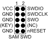
The ARM SWD interface is a subset of the JTAG interface, making use of TCK and TMS pins. The ARM JTAG and AVR JTAG connectors are, however, not pin-compatible, so when designing an application PCB, which uses a SAM device with SWD or JTAG interface, it is recommended to use the ARM pinout shown in the figure below. The SAM connector port on the Power Debugger can connect directly to this pinout.
The Power Debugger is capable of streaming UART-format ITM trace to the host computer. Trace is captured on the TRACE/SWO pin of the 10-pin header (JTAG TDO pin). Data is buffered internally on the Power Debugger and is sent over the HID interface to the host computer. The maximum reliable data rate is about 3MB/s.