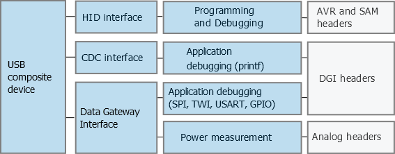
The Microchip Power Debugger hardware consists of three main sections; the debugger, analog front-end, and data gateway. The logical construction of the tool is shown here.
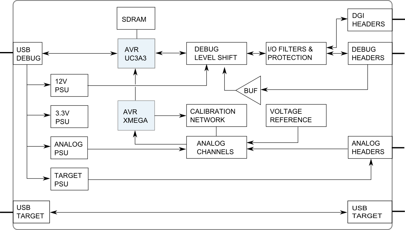
Power is supplied to the Power Debugger from the USB bus connected to the DEBUG port, regulated to 3.3V by a step-down switch-mode regulator. The VTG pins are used as a reference input-only, and a separate power supply feeds the variable-voltage side of the on-board level converters. At the heart of the Power Debugger main board is the Microchip AVR UC3 microcontroller AT32UC3A3256, which runs at up to 84 MHz depending on the tasks being processed. The microcontroller includes an on-chip USB 2.0 high-speed module, allowing high data throughput to and from the tool.