| Symbol | Parameter | Min. | Max | Units |
|---|---|---|---|---|
| VPP | Programming Enable Voltage | 11.5 | 12.5 | V |
| IPP | Programming Enable Current | - | 250 | μA |
| tDVXH | Data and Control Valid before XTAL1 High | 67 | - | ns |
| tXLXH | XTAL1 Low to XTAL1 High | 200 | - | ns |
| tXHXL | XTAL1 Pulse Width High | 150 | - | ns |
| tXLDX | Data and Control Hold after XTAL1 Low | 67 | - | ns |
| tXLWL | XTAL1 Low to WR Low | 0 | - | ns |
| tXLPH | XTAL1 Low to PAGEL high | 0 | - | ns |
| tPLXH | PAGEL low to XTAL1 high | 150 | - | ns |
| tBVPH | BS1 Valid before PAGEL High | 67 | - | ns |
| tPHPL | PAGEL Pulse Width High | 150 | - | ns |
| tPLBX | BS1 Hold after PAGEL Low | 67 | - | ns |
| tWLBX | BS2/1 Hold after RDY/BSY high | 67 | - | ns |
| tPLWL | PAGEL Low to WR Low | 67 | - | ns |
| tBVWL | BS1 Valid to WR Low | 67 | - | ns |
| tWLWH | WR Pulse Width Low | 150 | - | ns |
| tWLRL | WR Low to RDY/BSY Low | 0 | 1 | μs |
| tWLRH | WR Low to RDY/BSY High(1) | 3.2 | 3.4 | ms |
| tWLRH_CE | WR Low to RDY/BSY High for Chip Erase(2) | 9.8 | 10.5 | ms |
| tXLOL | XTAL1 Low to OE Low | 0 | - | ns |
| tBVDV | BS1 Valid to DATA valid | 0 | 350 | ns |
| tOLDV | OE Low to DATA Valid | - | 350 | ns |
| tOHDZ | OE High to DATA Tri-stated | - | 250 | ns |
Note:
- 1.tWLRH is valid for the Write Flash, Write EEPROM, Write Fuse bits and Write Lock bits commands.
- 2.tWLRH_CE is valid for the Chip Erase command.
Figure 1. Parallel Programming Timing,
Including some General Timing Requirements
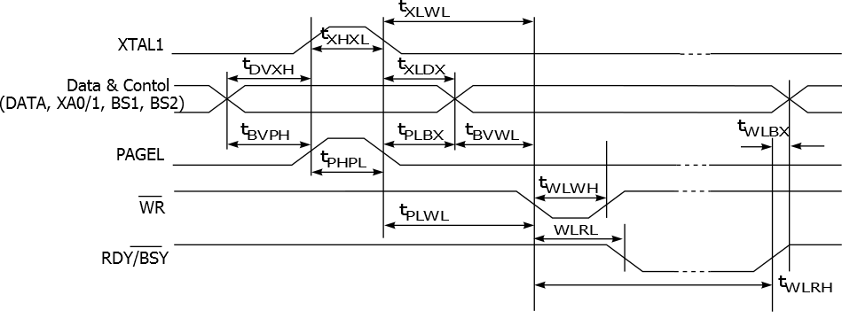
Figure 2. Parallel Programming Timing, Loading
Sequence with Timing Requirements
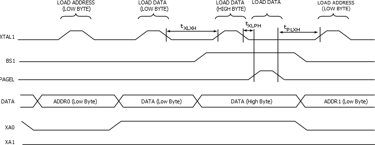
Note: The timing requirements shown in Parallel Programming Characteristics (i.e., tDVXH, tXHXL, and tXLDX) also
apply to loading operation
Figure 3. Parallel Programming Timing, Reading
Sequence (within the Same Page) with Timing Requirements
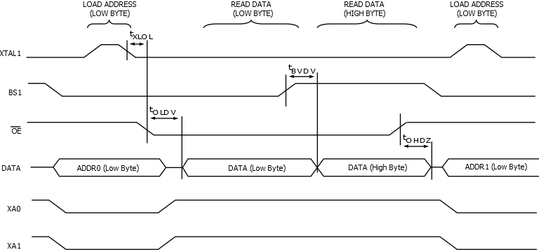
Note: The timing requirements shown in Parallel Programming Characteristics (i.e., tDVXH, tXHXL, and tXLDX) also
apply to reading operation.