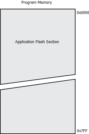
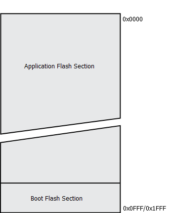
The device contains 4/8/16Kbytes On-chip In-System Reprogrammable Flash memory for program storage. Since all AVR instructions are 16 or 32 bits wide, the Flash is organized as 2/4/8K x 16. For software security, the Flash Program memory space is divided into two sections, Boot Loader Section and Application Program Section in ATmega88PB and ATmega168PB.
The Flash memory has an endurance of at least 10,000 write/erase cycles. The device Program Counter (PC) is 11/12/13 bits wide, thus addressing the 2/4/8K program memory locations.
Constant tables can be allocated within the entire program memory address space (see the LPM – Load Program Memory instruction description).
Timing diagrams for instruction fetch and execution are presented in Instruction Execution Timing.