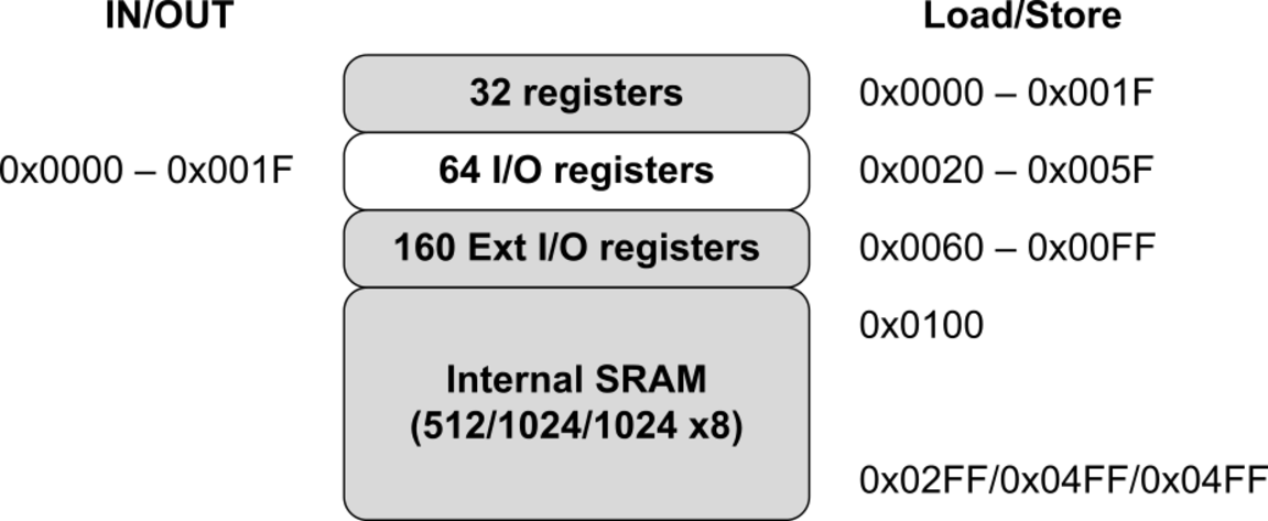
The following figure shows how the device SRAM Memory is organized.
The device is a complex microcontroller with more peripheral units than can be supported within the 64 locations reserved in the Opcode for the IN and OUT instructions. For the Extended I/O space from 0x60 - 0xFF in SRAM, only the ST/STS/STD and LD/LDS/LDD instructions can be used.
The lower 768/1280/1280 data memory locations address both the Register File, the I/O memory, Extended I/O memory, and the internal data SRAM. The first 32 locations address the Register File, the next 64 location the standard I/O memory, then 160 locations of Extended I/O memory, and the next 512/1024/1024 locations address the internal data SRAM.
- 1.Direct
- The direct addressing reaches the entire data space.
- 2.Indirect with Displacement
- The Indirect with Displacement mode reaches 63 address locations from the base address given by the Y- or Z-register.
- 3.Indirect
- In the Register File, registers R26 to R31 feature the indirect addressing pointer registers.
- 4.Indirect with Pre-decrement
- The address registers X, Y, and Z are decremented.
- 5.Indirect with Post-increment
- The address registers X, Y, and Z are incremented.
The 32 general purpose working registers, 64 I/O Registers, 160 Extended I/O Registers, and the 512/1024/1024 bytes of internal data SRAM in the device are all accessible through all these addressing modes.