This section describes the Instruction Set.
| Instruction/Operation | Instruction Format | |||
|---|---|---|---|---|
| Byte 1 | Byte 2 | Byte 3 | Byte 4 | |
| Programming Enable | 0xAC | 0x53 | 0x00 | 0x00 |
| Chip Erase (Program Memory/EEPROM) | 0xAC | 0x80 | 0x00 | 0x00 |
| Poll RDY/BSY | 0xF0 | 0x00 | 0x00 | data byte out |
| Load Instructions | ||||
| Load Extended Address byte(1) | 0x4D | 0x00 | Extended adr | 0x00 |
| Load Program Memory Page, High byte | 0x48 | 0x00 | adr LSB | high data byte in |
| Load Program Memory Page, Low byte | 0x40 | 0x00 | adr LSB | low data byte in |
| Load EEPROM Memory Page (page access) | 0xC1 | 0x00 | 0000 000aa(2) | data byte in |
| Read Instructions(5) | ||||
| Read Program Memory, High byte | 0x28 | adr MSB | adr LSB | high data byte out |
| Read Program Memory, Low byte | 0x20 | adr MSB | adr LSB | low data byte out |
| Read EEPROM Memory | 0xA0 | 0000 00aa(2) | aaaa aaaa(2) | data byte out |
| Read Lock bits(3) | 0x58 | 0x00 | 0x00 | data byte out |
| Read Signature Byte | 0x30 | 0x00 | 0000 000aa(2) | data byte out |
| Read Fuse bits(3) | 0x50 | 0x00 | 0x00 | data byte out |
| Read Fuse High bits(3) | 0x58 | 0x08 | 0x00 | data byte out |
| Read Extended Fuse Bits(3) | 0x50 | 0x08 | 0x00 | data byte out |
| Read Calibration Byte | 0x38 | 0x00 | 0x00 | data byte out |
| Write Instructions(5) | ||||
| Write Program Memory Page(6) | 0x4C | adr MSB(8) | adr LSB(8) | 0x00 |
| Write EEPROM Memory | 0xC0 | 0000 00aa(2) | aaaa aaaa(2) | data byte in |
| Write EEPROM Memory Page (page access) | 0xC2 | 0000 00aa(2) | aaaa aa00(2) | 0x00 |
| Write Lock bits(3)(4) | 0xAC | 0xE0 | 0x00 | data byte in |
| Write Fuse bits(3)(4) | 0xAC | 0xA0 | 0x00 | data byte in |
| Write Fuse High bits(3)(4) | 0xAC | 0xA8 | 0x00 | data byte in |
| Write Extended Fuse Bits(3)(4) | 0xAC | 0xA4 | 0x00 | data byte in |
Note:
- 1.Not all instructions are applicable for all parts.
- 2.a = address.
- 3.Bits are programmed ‘0’, unprogrammed ‘1’.
- 4.To ensure future compatibility, unused Fuses and Lock bits should be unprogrammed (‘1’) .
- 5.Refer to the corresponding section for Fuse and Lock bits, Calibration and Signature bytes and Page size.
- 6.Instructions accessing program memory use a word address. This address may be random within the page range.
Note: See http://www.microchip.com/design-centers/8-bit/microchip-avr-mcus for Application Notes regarding programming and programmers.
If the LSB in RDY/BSY data byte out is ‘1’, a programming operation is still pending. Wait until this bit returns ‘0’ before the next instruction is carried out.
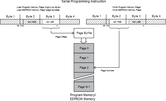
Within the same page, the low data byte must be loaded prior to the high data byte.
After data is loaded to the page buffer, program the EEPROM page, Please refer to the following figure.
Figure 1. Serial Programming Instruction
example