The Timer/Counter is a synchronous design
and the timer clock (clkT0) is
therefore shown as a clock enable signal in the following figures. If the given instance of
the TC0 supports an asynchronous mode, clkI/O should
be replaced by the TC oscillator clock.
The figures include information on when interrupt flags are set.
The first figure below illustrates timing data for basic Timer/Counter operation close to
the MAX value in all modes other than Phase Correct PWM mode.
Figure 1. Timer/Counter Timing Diagram, no
Prescaling
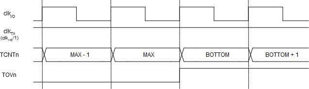
Note: The “n” in the register and bit names
indicates the device number (n = 0 for Timer/Counter 0), and the “x” indicates Output Compare unit (A/B).
The next figure shows the same timing data,
but with the prescaler enabled.
Figure 2. Timer/Counter Timing Diagram, with
Prescaler (fclk_I/O/8)
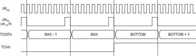
Note: The “n” in the register and bit names indicates the device number (n = 0 for Timer/Counter 0), and the “x”
indicates Output Compare unit (A/B).
The next figure shows the setting of OCF0B in all modes and OCF0A in all
modes (except CTC mode and PWM mode where OCR0A is TOP).
Figure 3. Timer/Counter Timing Diagram,
Setting of OCF0x, with Prescaler (fclk_I/O/8)
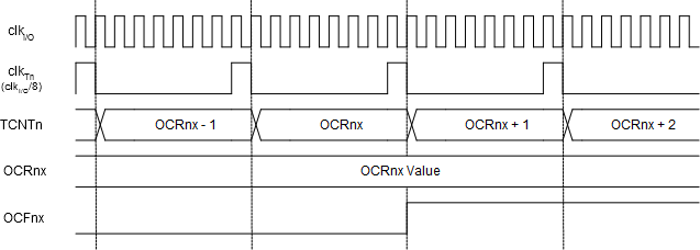
Note: The “n” in the register and bit names indicates the device number (n = 0 for Timer/Counter 0), and the “x”
indicates Output Compare unit (A/B).
The next figure shows the setting of OCF0A and the clearing of TCNT0 in CTC
mode and fast PWM mode where OCR0A is TOP.
Figure 4. Timer/Counter Timing Diagram, Clear
Timer on Compare Match mode, with Prescaler (fclk_I/O/8)
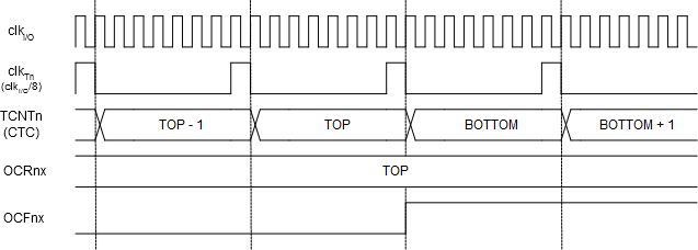
Note: The “n” in the register and bit names indicates the device number (n = 0 for Timer/Counter 0), and the
“x” indicates Output Compare unit (A/B).