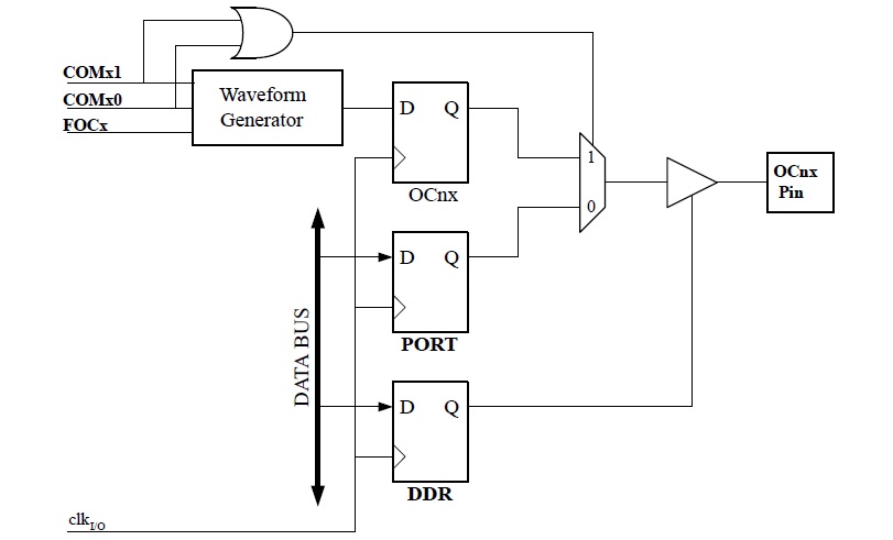
As the above figure shows, the OCnA,OCnB pin behavior depends on both COMx[1:0] bits settings in the TCCRnA register and compare output (OCnX) from waveform generator, which is controlled by the WGM[3:0] bits setting in the TCCRnA, TCCRnB registers. However, the OCnx pin direction (input or output) is still controlled by the Data Direction Register (DDR). For altering to compare output function, DDR_OCnx should be set output.
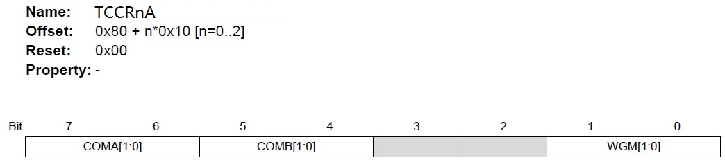
Bits 7:6 – COMA[1:0]: Compare Output Mode for Channel A [n = 1:0]
Bits 5:4 – COMB[1:0]: Compare Output Mode for Channel B [n = 1:0]
The COMA[1:0] and COMB[1:0] control the Output Compare pins (OCnA and OCnB respectively) behavior. If one or both of the COMA[1:0] bits are written to one, the OCnA output overrides the normal port functionality of the I/O pin it is connected to. If one or both of the COMB[1:0] bit are written to one, the OCnB output overrides the normal port functionality of the I/O pin it is connected to.
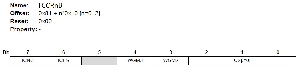
Bits [1:0] of TCCRnA + Bits [4:3] of TCCRnB– WGM[3:0] bits control the counting sequence of the counter, the source for maximum (TOP) counter value, and what type of waveform generation to be used. The table below shows the COMx[1:0] bits functionality when the WGM[3:0] bits are set to normal mode or CTC mode. For more detailed description, refer to the ATmega328PB datasheet.
| COMA1/COMB1 | COMA0/COMB0 | Description |
|---|---|---|
| 0 | 0 | Normal port operation, OCnA/OCnB disconnected |
| 0 | 1 | Toggle OCnA/OCnB on Compare Match |
| 1 | 0 | Clear OCnA/OCnB on Compare Match (set output to low level) |
| 1 | 1 | Set OCnA/OCnB on Compare Match (set output to high level) |