Figure 1. AT32UC3L-EK Programming and Debugging
Interface Logical View
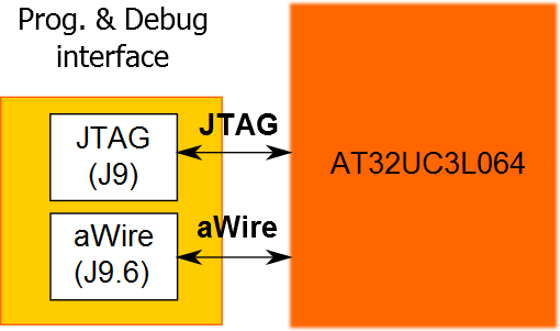
The main programming and debugging interface of the AT32UC3L-EK is meant to program and debug the AT32UC3L064. There are two debug interfaces available on the AT32UC3L064: the JTAG interface and the aWire interface (single pin debug system), both accessible through the J9 connector.
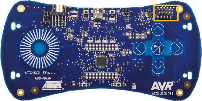
Note that there is another programming and debugging interface block on the kit, but it is related to the AT32UC3B1256 chip in charge of USB communication (refer to USB Interface).
Figure 2. AT32UC3L-EK Programming and Debugging
Interface Location