
6 Pseudo Random Number Generator Using the SPI Module
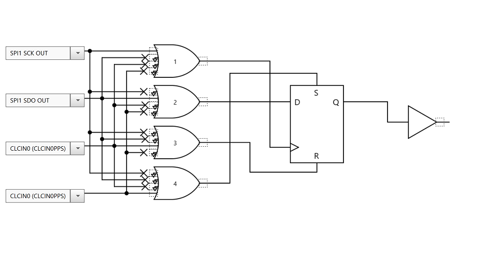
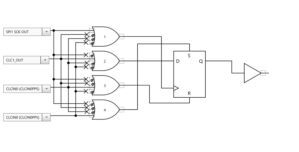
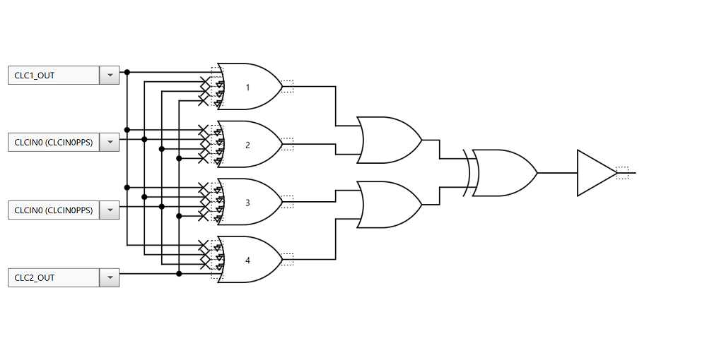
This example implements three CLCs for logic/flip-flops as well as the SPI
module as a shift register. Two CLCs are configured as D flip-flops with both S and R
tied to ‘0’, and the third is configured as an XOR gate. Both D
flip-flops use the SCK signal from the SPI module as their clock, and the first
flip-flop uses the SDO output of the SPI module as its D input. The second flip-flop
uses the Q output of the first flip-flop as its D input. The Q outputs of both
flip-flops are then XOR'ed together and fed back to the SPI module as the SDI input.
This circuit works by feeding an initial 8-bit seed value into the SPI transmit FIFO,
which the SPI will then send out onto the SDO signal. The CLC logic will then create a
new byte (bit-by-bit) and input that data back into the SPI module using the SDI input.
Doing this uses the original seeded value that was transmitted by the SPI module to
create a new random value that is transferred to the RXFIFO of the SPI module all in
hardware. The SPI module operates in Full-Duplex mode, meaning that it will transfer
data whenever the TXFIFO has been written and if the RXFIFO is not already full. Lastly,
the DMA module must be configured so that it transfers data from the RXFIFO to the
TXFIFO, which will allow the circuit to continuously generate psuedo-random numbers. The
configuration code for DMA and PPS settings can be found in DMA Initialization Code.
Pseudo Random Number Generator Initialization Code
/*This code block configures the CLCs
for Pseudo Random Number Generator.
  */

void CLC1_Initialize(void) {
    CLCSELECT = 0x00;           // SLCT 0
    CLCnPOL = 0x00;	      // Gate and CLCnOUT Output polarity Selection
    CLCnSEL0 = 0x41;            // D1S SPI1 SCK OUT
    CLCnSEL1 = 0x40;            // D2S SPI1 SDO OUT
    CLCnSEL2 = 0x00;            // D3S CLCIN0 (CLCIN0PPS)
    CLCnSEL3 = 0x00;            // D4S CLCIN0 (CLCIN0PPS)
    CLCnGLS0 = 0x02;            // CLCn Gate 1 Logic Selection
    CLCnGLS1 = 0x08;            // CLCn Gate 2 Logic Selection
    CLCnGLS2 = 0x20;            // CLCn Gate 3 Logic Selection
    CLCnGLS3 = 0x40;            // CLCn Gate 4 Logic Selection
    CLCDATA = 0x00;             // CLC1OUT 0
    CLCnCON = 0x84;             // EN enabled; INTN disabled; INTP disabled; MODE 1-input D flip-flop with S and R
}

void CLC2_Initialize(void) {
    CLCSELECT = 0x01;           // SLCT 1
    CLCnPOL = 0x00;             // Gate and CLCnOUT Output polarity Selection
    CLCnSEL0 = 0x41;            // D1S SPI1 SCK OUT
    CLCnSEL1 = 0x33;            // D2S CLC1_OUT
    CLCnSEL2 = 0x02;            // D3S CLCIN2 (CLCIN2PPS)
    CLCnSEL3 = 0x00;            // D4S CLCIN0 (CLCIN0PPS)
    CLCnGLS0 = 0x02;            // CLCn Gate 1 Logic Selection
    CLCnGLS1 = 0x08;            // CLCn Gate 2 Logic Selection
    CLCnGLS2 = 0x20;            // CLCn Gate 3 Logic Selection
    CLCnGLS3 = 0x40;            // CLCn Gate 4 Logic Selection
    CLCDATA = 0x00;             // CLC2OUT 0;
    CLCnCON = 0x84;             // EN enabled; INTN disabled; INTP disabled; MODE 1-input D flip-flop with S and R;
}

void CLC3_Initialize(void) {
    CLCSELECT = 0x02;           // SLCT 2
    CLCnPOL = 0x00;             // Gate and CLCnOUT Output polarity Selection
    CLCnSEL0 = 0x33;            // D1S CLC1_OUT;
    CLCnSEL1 = 0x00;            // D2S CLCIN0 (CLCIN0PPS);
    CLCnSEL2 = 0x00;            // D3S CLCIN0 (CLCIN0PPS);
    CLCnSEL3 = 0x34;            // D4S CLC2_OUT;
    CLCnGLS0 = 0x02;            // CLCn Gate 1 Logic Selection
    CLCnGLS1 = 0x08;            // CLCn Gate 2 Logic Selection
    CLCnGLS2 = 0x00;            // CLCn Gate 3 Logic Selection
    CLCnGLS3 = 0x40;            // CLCn Gate 4 Logic Selection
    CLCDATA = 0x00;             // CLC3OUT 0;
    CLCnCON = 0x81;             // EN enabled; INTN disabled; INTP disabled; MODE OR-XOR;
}
DMA Initialization Code
/*This code block configures the DMA
and PPS Settings for Pseudo Random Number Generator.
  */

void DMA1_Initialize(void) {
    DMASELECT = 0x00;           // Select DMA1
    DMAnSSA = &SPI1RXB;         // Source is SPI1 RX Buffer
    DMAnDSA = &SPI1TXB;         // Destination is SPI1 TX Buffer
    DMAnCON1 = 0x0B;            // DMODE unchanged, SMODE increments, SIRQEN cleared upon reload
    DMAnSSZ = 0x01;             // Source size is one (one buffer to write)
    DMAnDSZ = 0x01;             // Destination size is one (one buffer to write)
    DMAnSIRQ = 0x18;            // DMA Transfer Trigger Source = SPI1RXIF
    DMAnAIRQ = 0x14;            // DMA Transfer Abort Source = DMA1SCNTIF

    PIR2bits.DMA1SCNTIF = 0;    // Clear Source Count Interrupt Flag bit
    PIR2bits.DMA1AIF = 0;       // Clear abort Interrupt Flag bit
    PIE2bits.DMA1AIE = 1;       // Enable abort Interrupt

    asm("BCF INTCON0,7");       // Lock the prority
    asm ("BANKSEL PRLOCK");
    asm ("MOVLW 0x55");
    asm ("MOVWF PRLOCK");
    asm ("MOVLW 0xAA");
    asm ("MOVWF PRLOCK");
    asm ("BSF PRLOCK, 0");
    asm("BSF INTCON0,7");
}

// PPS Settings
    RC3PPS = 0x00;              // RC3->SPI1:SCK1
    CLCIN0PPS = 0x10;           // RC0->CLC3:CLCIN0;  Must connect to GND
    RB0PPS = 0x03;              // RB0->CLC3:CLC3_out
    SPI1SDIPPS = 0x08;          // RB0->SPI1:SDI1;  Connects to CLC3_out

    SPI1TXB = 0x2C;             // Load SPI1TXB with beginning 'seed' value