
3 Servicing Peripheral Interrupts While Writing Flash
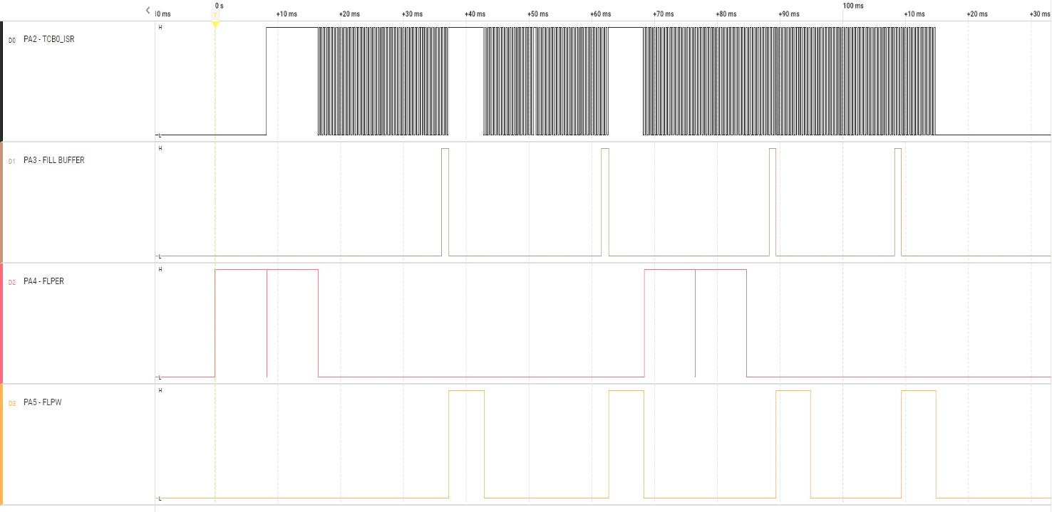
This example shows the advantage of writing to the RWW Flash section from the NRWW Flash section. It is easy to get an overview of code flow and how it works with an oscilloscope or logic analyzer by using device pins for interrupt events and different memory statuses.
Testing
The program memory is divided into smaller pieces called pages. Each page is written and erased separately and consists of several bytes. The Flash has page granularity for the AVR EA, meaning it will perform an erase and/or write for every byte in the page whenever a change is necessary. In comparison, the EEPROM memory has byte granularity and can erase and write single bytes at a time.
The code works by first erasing the pages where data will be saved, filling up a buffer, and then performing a page write using the buffer values. A periodic timer interrupt continuously populate the buffer.
When the ring buffer is filled with new data >= PROGMEM_PAGE_SIZE, it
copies the PROGMEM_PAGE_SIZE number of bytes from the ring buffer to the
Flash page buffer and starts a Flash page write. It repeats this process a second time.
Writing to the Capture/Compare (CCMP) register in the TCB timer/counter changes the ISR period.
The code toggles some status pins, which makes it possible to scope the program flow:
PA2_ISRtoggles every time the TCB0 periodic interrupt ISR is handledPA3_Bufferis high when the Flash page buffer is being loadedPA4_FLPERis high while the Flash page erase is ongoingPA5_FLPWis high while the Flash page write is ongoing
As the application runs through its state machine, these pins will toggle, as seen in the image below. A more detailed description of this flow can be seen in the examples “README” file.
Understanding The Code
The linked code examples come in two flavors - an MPLAB X studio using MCC to generate drivers and a bare-metal project created in Microchip Studio. The projects have the same code flow and are divided into the following parts:
- Main file and function
- Timer 0 - Filling buffer
- Timer 1 - Switch debounce
- NVM controller
FUSES =
{
    .SYSCFG0 = FUSE_SYSCFG0_DEFAULT,
    .SYSCFG1 = FUSE_SYSCFG1_DEFAULT,

    .WDTCFG = FUSE_WDTCFG_DEFAULT,
    .BODCFG = FUSE_BODCFG_DEFAULT,
    .OSCCFG = FUSE_OSCCFG_DEFAULT,

    .BOOTSIZE = 31,    // 0x0000 -> 0x1F00 : BOOT Section
    .CODESIZE = 1,     // 0x01F00 -> FLASH_END : APPDATA Section
};
Most fuses are set to their default value, except BOOTSIZE, which is set to 31
blocks of 256 bytes and CODESIZE. As CODESIZE is set to 1, the program memory is logically
split between the BOOT and APPDATA section.Main file and setup
The main file of the system contains the initialization and main structure of the examples. The important things to notice are how the RWW/NRWW sections are defined and that the interrupt vector table is moved to the start of the BOOT section. Lastly, the mapped program memory points to the first section (the location of the .nrww_program, .nrww_data, and .rww_data sections). These initializations ensures that running code only exists in the program memory’s NRWW section and that there exists memory addresses both in RWW and NRWW sections for data.
// TCB with capture interrupt
TCB0.INTCTRL = TCB_CAPT_bm;
TCB0.CCMP = TOP_VALUE;
TCB0.CTRLA = TCB_CLKSEL_DIV1_gc;
This timer is set up as a periodic interrupt that will trigger on capture when active. Note that the initialization does not enable the timer. The interrupt routine fills up the data buffer when called, as seen below.
// TCB0 capture interrupt
FillBuffer();
// Clear intflag
TCB0.INTFLAGS = TCB_CAPT_bm;
Timer 1
// TCB with periodic interrupt
TCB1.INTCTRL = TCB_CAPT_bm;
TCB1.CCMP = TCB1_TOP_VALUE;
TCB1.CTRLA = TCB_CLKSEL_DIV1_gc | TCB_ENABLE_bm;
// TCB1 capture interrupt
DebounceSW0();
// Clear intflag
TCB1.INTFLAGS = TCB_CAPT_bm;
Erasing the Program Memory
NRWW_DATA_last_addr = ((((uint16_t) &nrww_array) & 0x7FFF) + MAPPED_PROGMEM_START + DATA_SIZE);

while ((uint16_t)nrwwFlashPointer < NRWW_DATA_last_addr)
{
    _PROTECTED_WRITE_SPM(NVMCTRL.CTRLA, NVMCTRL_CMD_NOCMD_gc);

    // Perform a dummy write to this address to update the address register in NVMCTL
    *nrwwFlashPointer = 0;

    _PROTECTED_WRITE_SPM(NVMCTRL.CTRLA, NVMCTRL_CMD_FLPER_gc);

    while (NVMCTRL.STATUS & NVMCTRL_FLBUSY_bm)
    {
        ; // wait for Flash erase to complete
    }
    SCOPE_PORT.OUTCLR = SCOPE_FLPER_bm;

    nrwwFlashPointer = nrwwFlashPointer + PROGMEM_PAGE_SIZE;
}
The Flash erase operation for NRWW and RWW data sections is the same. It begins by setting the Flash page buffer to the area that will be erased. The FLPER pin is driven HIGH, so it's possible to see on the scope when the Flash erase operation is about to start. It sends NOCMD instructions to the NVM Controller to clear the previous NVM command to avoid a command collision error and is followed by a dummy write/store. The page erase command is sent to the NVM Controller. FLPER pin is driven LOW once the NVMCTRL.STATUS register shows that the Flash is not busy and the address of the next erase is incremented by a page size. The Flash erase operation is complete once the data section has been written to.
Writing the Program Memory
// Check if we have a full page to fill
if ((writeIndex - readIndex) >= PROGMEM_PAGE_SIZE)
{
    _PROTECTED_WRITE_SPM(NVMCTRL.CTRLA, NVMCTRL_CMD_NOCMD_gc);

    for (uint8_t i = 0; i < PROGMEM_PAGE_SIZE; i++)
    {
        *nrwwFlashPointer++ = buffer[readIndex++];
    }
    SCOPE_PORT.OUTCLR = SCOPE_BUFFER_bm;
    SCOPE_PORT.OUTSET = SCOPE_FLPW_bm;

    // Write the Flash page
    _PROTECTED_WRITE_SPM(NVMCTRL.CTRLA, NVMCTRL_CMD_FLPW_gc);
    while (NVMCTRL.STATUS & NVMCTRL_FLBUSY_bm)
    {
        ; // wait Flash write page operation to complete
    }
}
The Flash programming operation for NRWW and RWW data sections is the same. It begins by checking if enough data are available to write to a full Flash page. If not, it will wait until enough data have been generated. If yes, it sends NOCMD instructions to the NVM Controller to clear the previous NVM command to avoid a command collision error. Afterward, the BUFFER pin is driven HIGH, so it's possible to use the scope to see when the buffer load operation is about to start. Data is being read from the data buffer and stored in the Flash page buffer. When the equivalent of a complete page has been read and stored, the BUFFER pin is driven LOW. The FLPW pin is driven HIGH, and the page write command is sent to the NVM Controller. FLPW pin is driven LOW once the NVMCTRL.STATUS register shows that the Flash is not busy and the address of the next page write is incremented by a page size. The Flash write operation is complete once the data section has been written to.
For the erase and write functions above, the code snippets are from the bare metal example and will be formatted differently for the MCC example. However, the functionality will be the same for each example.
Filling the buffer
void FillBuffer(void)
{
    // Fill the buffer with some data
    SCOPE_PORT.OUTTGL = SCOPE_ISR_bm;
    buffer[writeIndex++] = (data >> 2);
    data++;

    // Check if we have a buffer overflow
    if (writeIndex == readIndex)
    {
        // Overflow
        SCOPE_PORT.OUTTGL = SCOPE_OVERFLOW_bm;
    }
}
The FillBuffer function is triggered by the periodic interrupt on timer 0 when the timer compare counter reaches the set TOP value. The ISR pin toggles and the buffer is filled with data. OVERFLOW toggles if the buffer overflows.
SW0 Operation and Debouncing
The erase and write operation for both the NRWW and RWW data sections is started by a SW0 press. Subsequent SW0 presses will trigger the same process. The value of the last data location in the RWW data section is used as a seed for the new data. Due to this behavior, when SW0 is pressed and the program memory read, the user can observe a change in NRWW and RWW data sections. As a confirmation that SW0 has been pressed, LED0 lights up. It is necessary to trigger the whole operation of the example by a button press, as one needs to set up the external instruments (oscilloscope and/or logic analyzer) that can capture the toggling of the instrumentation pins. A simple debounce algorithm has been chosen and implemented. TCB1 is being employed for this purpose. Software debouncing the physical switch SW0 prevents the unwanted triggering of the erase and write operations. Please note that the programming Flash has a limited erase/write endurance beyond which operation is not guaranteed (consult the device’s electrical characteristics for further information and details).
Moving the interrupt vector table
The vector interrupt placement depends on the Interrupt Vector Select (IVSEL) bit value in the Control A (CPUINT.CTRLA) register. If using no interrupt source, regular program code may be placed in these locations. By writing 1 to the IVSEL, the interrupt vector is placed at the start of the BOOT section of the Flash, enabling the interrupts to run as normal while an erase/write operation in the RWW section is running. As stated in the overview section, the syntax "RWW section" refers to which section is being programmed (erased or written) and not the one read. Only code located inside the NRWW Flash can be accessed by either executing a CPU instruction or reading data while the RWW section is being programmed.