4 Hardware Implementation
LED, Mechanical Switch, Power Supply, Crystal.
4.1 Crystal
| ATtiny3227 Pin | Function | Shared Functionality |
|---|---|---|
| PB3 | TOSC1 | Edge connector |
| PB2 | TOSC2 | Edge connector |
- The two I/O lines routed to the edge connector must be disconnected to reduce the chance of contention to the crystal and to remove excessive capacitance on the lines
- Disconnect the edge connector by cutting the two cut straps on the bottom side of the board, J107 and J108. Marked PB2 and PB3 in the silkscreen.
- Connect the crystal by soldering on a solder blob on each circular solder point next to the crystal on the top side of the board, J109 and J110
- Add suitable capacitors to C102 and C103
The crystal has a cut strap (J111), which can be used to measure the oscillator safety factor and is done by cutting the strap and adding a 0402 SMD resistor across the strap. The AN2648 application note from Microchip contains more information about oscillator allowance and safety factors.
4.2 LED
One yellow user LED is available on the ATtiny3227 Curiosity Nano board. Either GPIO or PWM can control it. Driving the connected I/O line to GND can also activate the LED.
| ATtiny3227 Pin | Function | Shared Functionality |
|---|---|---|
| PB7 | Yellow LED0 | Edge connector, On-board debugger |
4.3 Mechanical Switch
The ATtiny3227 Curiosity Nano board has one mechanical switch - a generic user-configurable switch. Pressing it will connect the I/O pin to ground (GND).
| ATtiny3227 Pin | Description | Shared Functionality |
|---|---|---|
| PC4 | User switch (SW0) | Edge connector, On-board debugger |
4.4 Power Supply
The USB port powers the board. The VBUS net is limited to a 2 V/ms slew rate and is current limited to 500 mA by U202 (MIC2008).
The power supply consists of two LDO regulators, one to generate 3.3V for the on-board debugger and an adjustable LDO regulator for the target ATtiny3227 microcontroller and its peripherals. The voltage from a USB connector can vary between 4.4V and 5.25V (according to the USB specification) and will limit the maximum voltage supplied to the target. The figure below shows the entire power supply system on the ATtiny3227 Curiosity Nano.
4.4.1 Cut Straps
- Target Power Strap (J201)
- Power Supply Strap (J200)
- Debugger Pins (J101, J102, J103, J104, J105, J106)
4.4.2 Target Regulator
The target voltage regulator is a MIC5353 variable output LDO. The on-board debugger can adjust the voltage output supplied to the board target section by manipulating the MIC5353’s feedback voltage. The hardware implementation is limited to an approximate voltage range from 1.7V to 5.1V. Additional output voltage limits are configured in the debugger firmware to ensure that the output voltage never exceeds the hardware limits of the ATtiny3227 microcontroller. The voltage limits configured in the on-board debugger on ATtiny3227 Curiosity Nano are 1.8–5.5V.
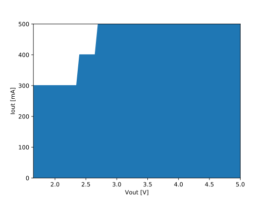
MIC5353 supports a maximum current load of 500 mA. It is an LDO regulator in a small package placed on a small printed circuit board (PCB) and can reach the thermal shutdown condition at lower loads than 500 mA. The maximum current load depends on the input voltage, the selected output voltage, and the ambient temperature. The figure below shows the safe operating area for the regulator, with an input voltage of 5.1V and an ambient temperature of 23°C.
The voltage output of the target regulator is continuously monitored (measured) by the on-board debugger. An error condition will be flagged - and the target voltage regulator will be switched off, detecting and handling any short-circuit conditions if it is more than 100 mV over/under the set device voltage. It will also detect and handle if an external voltage, which causes VCC_TARGET to move outside the voltage setting monitoring window of ±100 mV, is suddenly applied to the VTG pin without setting the VOFF pin low.
4.4.3 External Supply
Instead of the on-board target regulator, an external voltage can power the ATtiny3227 Curiosity Nano. When shorting the Voltage Off (VOFF) pin to the ground (GND) pin, the on-board debugger firmware disables the target regulator, and it is safe to apply an external voltage to the VTG pin.
It is also safe to apply an external voltage to the VTG pin when no USB cable is plugged into the DEBUG connector on the board.
The VOFF pin can be tied low/let go at any time, which will be detected by a pin-change interrupt to the on-board debugger, which controls the target voltage regulator accordingly.
Programming, debugging, and data streaming are still possible with an external power supply. The USB cable will power the debugger and signal level shifters. Both regulators, the debugger, and the level shifters are powered down when the USB cable is removed.
4.4.4 Power Supply Exceptions
This section summarizes most issues that can arise with the power supply.
Target Voltage Shuts Down
Not reaching the set target voltage can happen if the target section draws too much current at a given voltage, causing the thermal shutdown safety feature of the MIC5353 regulator to kick in. To avoid this, reduce the current load of the target section.
Target Voltage Setting is Not Reached
The USB input voltage (specified to be 4.4-5.25V) limits the maximum output voltage of the MIC5353 regulator at a given voltage setting and current consumption. If a higher output voltage is needed, use a USB power source with a higher input voltage or use an external voltage supply on the VTG pin.
Target Voltage is Different From Setting
An externally applied voltage to the VTG pin without setting the VOFF pin low can cause this. If the target voltage fluctuates by over 100 mV over/under the voltage setting, the on-board debugger will detect it, and the internal voltage regulator will shut down. To fix this issue, remove the applied voltage from the VTG pin, and the on-board debugger will enable the on-board voltage regulator when the new condition is detected. Note that the PS LED will blink rapidly if the target voltage is below 100 mV of the setting but will ordinarily turn on when it is more than 100 mV above it.
No, or Very Low Target Voltage and PS LED is Blinking Rapidly
A full or partial short circuit can cause this and is a particular case of the issue above. Remove it, and the on-board debugger will re-enable the on-board target voltage regulator.
No Target Voltage and PS LED is Lit 1
This situation occurs if the target voltage is set to 0.0V. To fix this, set the target voltage to a value within the specified voltage range for the target device.
No Target Voltage and PS LED is Lit 2
This situation can be an issue when cutting power jumper J200 and/or J201 and setting the target voltage regulator to a value within the specified voltage range for the target device. To fix this, solder a wire/bridge between the pads for J200/J201 or add a jumper on J201 if a pin header is mounted.
VBUS Output Voltage is Low or Not Present
If the VBUS output voltage is low or missing, the reason is probably a high-current drain on VBUS, and the current limit set by U202 (MIC2008) is tripped and has cut off VBUS completely. Reduce the current consumption on the VBUS pin to fix this issue.
4.4.5 Low-Power Measurement
Power to the ATtiny3227 comes from the on-board power supply and VTG pin through a 100 mil pin header marked with “POWER” in silkscreen (J201). To measure the power consumption of the ATtiny3227 and other peripherals connected to the board, cut the Target Power strap (J201) on the bottom side and connect an ammeter across it.
- Cut the POWER strap with a sharp tool.
- Solder a 1x2 100 mil pin header in the footprint.
- Connect an ammeter to the pin header.
- Write firmware that:
- Tri-states any I/O connected to the on-board debugger.
- Sets the microcontroller in its lowest Power sleep mode.
- Program the firmware into the ATtiny3227.
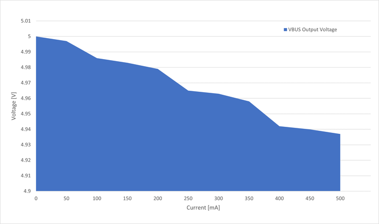
4.4.6 VBUS Output Pin
ATtiny3227 Curiosity Nano has a VBUS output pin that can be used to power external components that need a 5V supply. The VBUS output pin is protected by the same start-up delay with a slew rate and current limiter as the rest of the power supply. A side effect is a voltage drop on the VBUS output with higher current loads. The chart below shows the VBUS output voltage versus the current load of the VBUS output.