Unless otherwise noted, controlling dimensions are in inches; metric equivalents are shown for general information.
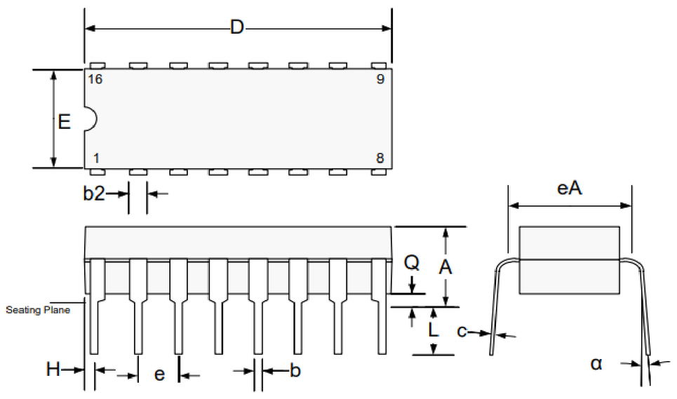
Figure 7-1. J 16-Pin Ceramic Dip
Dim.1
Millimeters
Inches
Min.
Max.
Min.
Max.
A
—
5.08
—
0.200
b
0.38
0.51
0.015
0.020
b2
1.04
1.65
0.045
0.065
c
0.20
0.38
0.008
0.015
D
19.30
19.94
0.760
0.785
E
5.59
7.11
0.220
0.280
e
2.54 BSC
0.100 BSC
eA
7.37
7.87
0.290
0.310
H
0.63
1.78
0.025
0.070
L
3.18
5.08
0.125
0.200
α
—
15°
—
15°
Q
0.51
1.02
0.020
0.040
Note:
Dimensions do not include protrusions; these shall not exceed 0.155 mm (.006”)
on any side. Lead dimension shall not include solder coverage.
BSC: Basic spacing between centers
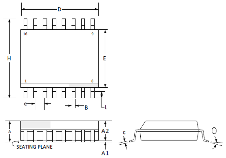
Figure 7-2. DW 16-Pin Plastic Wide-Body SOIC
Dim.1,2
Millimeters
Inches
Min.
Max.
Min.
Max.
A
2.06
2.65
0.081
0.104
A1
0.10
0.30
0.004
0.012
A2
2.03
2.55
0.080
0.100
B
0.33
0.51
0.013
0.020
c
0.23
0.32
0.009
0.013
D
10.08
10.50
0.397
0.413
E
7.40
7.60
0.291
0.299
e
1.27 BSC
0.05 BSC
H
10.00
10.65
0.394
0.419
L
0.40
1.27
0.016
0.050
Θ
0°
8°
0°
8°
LC3
—
0.10
—
0.004
Note:
Controlling dimensions for this package are in mm; inches are for reference
only
Dimensions shall not include mold flash or protrusions; these shall not exceed
0.155 mm (.006 in) on any side. Lead dimension shall not include solder
coverage.
Lead coplanarity
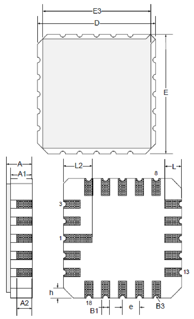
Figure 7-3. 20-Pin Ceramic Leadless Chip Carrier
Dim.1
Millimeters
Inches
Min.
Max.
Min.
Max.
D/E
8.64
9.14
0.340
0.360
E3
—
8.128
—
0.320
e
1.270 BSC
0.050 BSC
B1
0.635 TYP
0.025 TYP
L
1.02
1.52
0.040
0.060
A
1.626
2.286
0.064
0.090
h
1.016 TYP
0.040 TYP
A1
1.372
1.68
0.054
0.066
A2
—
1.168
—
0.046
L2
1.91
2.41
0.075
0.095
B3
0.203R
0.008R
Note:
All exposed metalized area shall be gold plated 60 micro-inch minimum
thickness over nickel plated unless otherwise specified in purchase order
DS00006622A
The online versions of the documents are provided as a courtesy. Verify all content and data in the device’s PDF documentation found on the device product page.