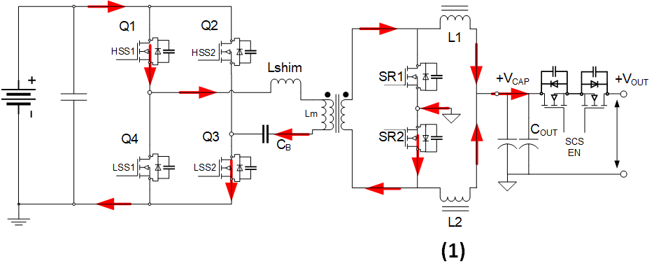
3.1 Phase-Shifted Full-Bridge with Current Doubler Rectifier
The Phase-Shifted Full-Bridge topology consists of a full bridge at the primary producing bipolar drive voltage for the SMPS transformer. The main function of the transformer is to provide required galvanic isolation and provide a step-down ratio. On the secondary, the Current Doubler Rectifier stage is implemented by using two low-side rectifiers and two output inductors; each SR leg running interleaved depending on the transformer pulse polarity.
The Phase-Shifted Full-Bridge topology works by having both primary side legs switching at 50% duty cycle with dead time (160ns for this design). There is no direct duty cycle variation, but rather a phase shift is introduced which produces bipolar voltage pulses for the Main Switch mode transformer. The phase-shift control range for this design is Ø = 0⁰ to 171⁰, resulting in 0 to 95% duty control. Additionally, an external shim inductance may be added to enforce ZVS at a given operating point.
|
|
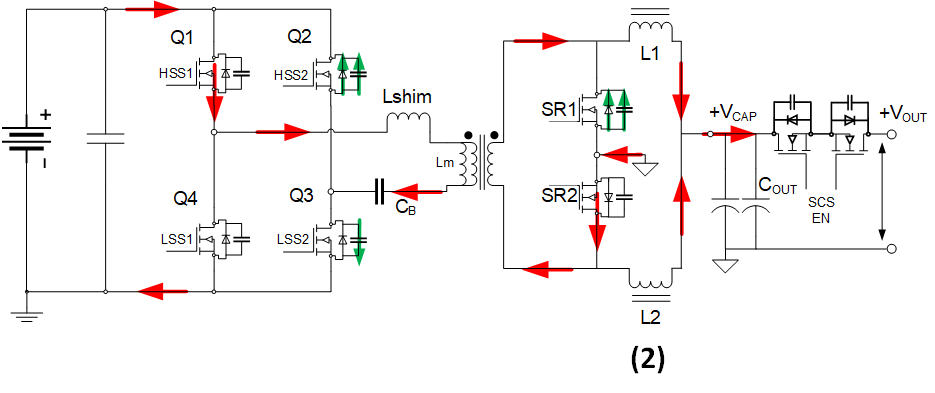
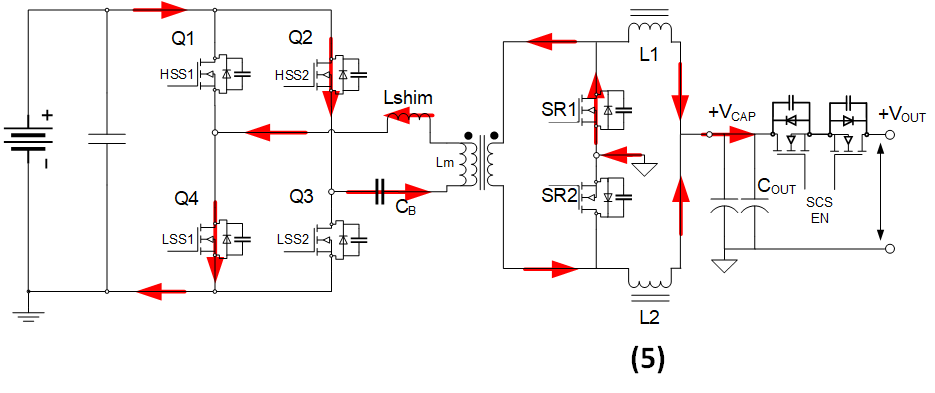
PHASE-1: Q1, Q3 diagonal is in an ON state and is conducting. This applies +VIN at XFR. Q2, Q4 are in an OFF state. SR2 is in an ON state and is conducting. SR1 is in an OFF state. L1, L2 conduct Io/2 current. SR2 conducts roughly Io during this phase. |
|
|
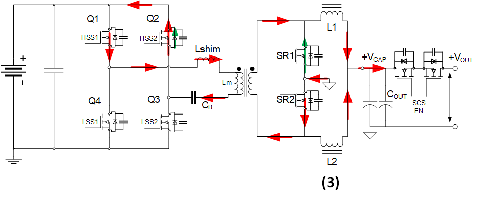
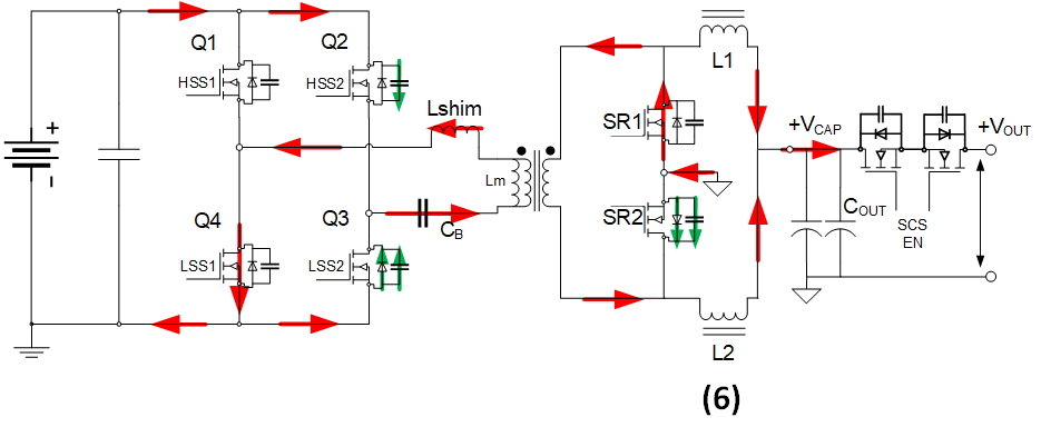
PHASE-2: Q1 is in an ON state. Q3 is switched OFF. Coss of Q3 charges. Current starts to flow through the Q2 body diode and discharges Q2 Coss. XFR primary voltage swings to 0V. SR2 is in an ON state and is conducting. Current starts to flow through the SR1 Body diode and discharges SR1 Coss. |
|
|
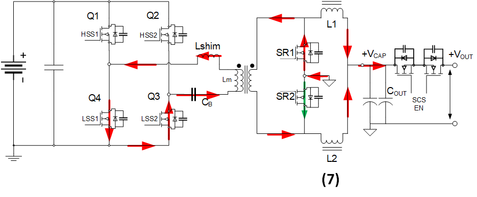
PHASE-3: Q1 is in an ON state. Q2 is switched ON with ZVS. Q4 and Q3 are in an OFF state. XFR primary Voltage becomes 0V, and the XFR current becomes constant as circulating currents. (Decreases slowly showing circulating losses.) SR2 is still conducting approximately Io. XFR secondary current does not change. SR1 is switched ON with ZVS and ZCS. |
|
|
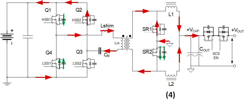
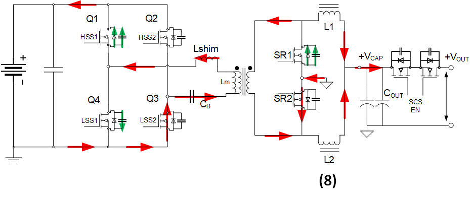
PHASE-4: Q2 is in an ON state. Q1 is switched OFF. Q1 Coss charges. Current starts flowing through the Q4 body diode and discharges Coss. XFR primary voltage swings towards negative VIN. SR2 is switched OFF, and SR1 is now conducting approximately Io. |
|
|
PHASE-5: Q2 is in an ON state. Q4 is switched ON. Q1 and Q3 are OFF. XFR primary voltage is now -VIN. SR2 body diode is reverse biased. SR1 is ON and conducting Io. |
|
|
PHASE-6: Q4 is ON and conducting. Q2 is switched OFF. Q2 Coss discharges and current starts to flow through Q3 body diode and Coss is discharged. XFR primary voltage swings to 0V. SR1 is in an ON state and is conducting. Current starts to flow through the SR2 Body diode and discharges Coss. |
|
|
PHASE-7: Q4 is in an ON state. Q3 is switched ON with ZVS. Q1 and Q2 are in an OFF state. XFR primary Voltage becomes 0V, and XFR current becomes constant as circulating currents. (Decreases slowly showing circulating losses.) SR1 is still conducting approximately Io. The XFR secondary current does not change. SR2 is switched ON with ZVS and ZCS. |
|
|
PHASE-8: Q3 is in an ON state. Q4 is switched OFF. Q4 Coss charges. Current starts flowing through the Q1 body diode and discharges Coss. XFR primary voltage swings towards positive VIN. SR1 is switched OFF, and SR2 is now conducting approximately Io. |