4 LIN Responder Basic Demo
This section provides a basic LIN communication between an 8-bit Curiosity Nano (CNANO) as Responder and the APG LIN Serial Analyzer as Commander.
4.1 Hardware Setup
- Refer to 8-bit Curiosity Nano Boards for the complete set of supported CNANO boards.
Configure the hardware as shown below. Plug the ATA663254 click to the mikroBUS® socket 1 of the CNANO base.

An example setup is shown below. The CNANO board and LIN Serial Analyzer are connected to the PC via USB. The LIN Serial Analyzer is powered by a 9V supply.

4.2 Software Environment
Download and install the following software:
4.3 Demo Network
This demo utilizes the readily-available LED (LED0) and push button switch (SW0) from the CNANO board.
| Frame | ID | Length (Bytes) | Signals | Publisher | Subscriber |
|---|---|---|---|---|---|
LED_Blink | 0x00 | 2 | Bit[15:0] Blink_Period | LIN Analyzer | CNANO |
Switch_Status | 0x01 | 1 | Bit[0] SW_State | CNANO | LIN Analyzer |
Error_Status | 0x3B | 1 | Bit[0] CNANO_ErrBit | CNANO | LIN Analyzer |
Blink_Period represents the 16-bit toggle period of LED0 in milliseconds.
SW_State returns the status of SW0 while
CNANO_ErrBit is the 1-bit response error signal required in LIN
2.x.
4.4 MCC Melody Configuration
The following instructions will walk the user through the steps for setting up a LIN Responder node’s peripherals, frames and signals.
4.4.1 Loading the Library
- Click the Content Manager button next to Device Resources. This will open the MCC Content Manager window.
- Under the Content Libraries tab, go to Libraries>LIN>LIN Responder. Select the latest version and hit the Apply button. The Melody windows will automatically refresh.
- Under Device Resources, select Libraries>LIN>LIN Responder. The LIN Responder can now be found under Project Resources.
The user has two options from here: manually configure the node attributes and frames, or use an LDF. To configure without an LDF, continue with Manual Configuration. To configure with an LDF, proceed to Configuration with LDF .
4.4.2 Manual Configuration (No LDF)
- Click the LIN Responder block in the Application Builder tab. This can also be done by going to Project Resources>Libraries>LIN>LIN Responder.
In the LIN Responder GUI, go to the Frames tab and add the following signals and frames:
Figure 4-3. Manual Frames Configuration 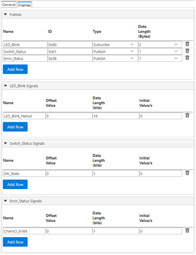
Go to the General tab and configure the fields as shown below
Figure 4-4. Manual Node Configuration 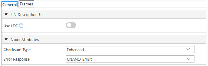
4.4.3 Configuration With LDF
If manual configuration has already been done, skip this section and proceed to Frame Processor Configuration.
- Copy and paste the below LDF to a text editor.
Save the file with an
.ldfextension.LIN_description_file; LIN_protocol_version = "2.2"; LIN_language_version = "2.2"; LIN_speed = 19.2 kbps; Nodes { Master: LIN_Analyzer, 1 ms, 0 ms ; Slaves: CNANO ; } Signals { LED_Blink_Period: 16, 0, LIN_Analyzer, CNANO ; SW_State: 1, 0, CNANO, LIN_Analyzer ; CNANO_ErrBit: 1, 0, CNANO, LIN_Analyzer ; } Frames { LED_Blink: 0, LIN_Analyzer, 2 { LED_Blink_Period, 0 ; } Switch_Status: 1, CNANO, 1 { SW_State, 0 ; } Error_Status: 59, CNANO, 1 { CNANO_ErrBit, 0 ; } } Node_attributes { CNANO{ LIN_protocol = "2.2" ; configured_NAD = 0xFF ; initial_NAD = 0xFF ; product_id = 0x0, 0x0, 255 ; response_error = CNANO_ErrBit ; P2_min = 50 ms ; ST_min = 0 ms ; N_As_timeout = 1000 ms ; N_Cr_timeout = 1000 ms ; configurable_frames { LED_Blink ; Switch_Status ; Error_Status ; } } } Schedule_tables { Demo_Sched { LED_Blink delay 5 ms ; Switch_Status delay 10 ms ; Error_Status delay 10 ms ; } }
- Click the LIN Responder block in the Application Builder to open the LIN Responder configuration window. This can also be done by going to Project Resources>Libraries>LIN>LIN Responder.
- Enable Use LDF
-
Click Select File and load the LDF
Figure 4-5. Node Settings Example Using LDF 
- Select “CNANO” as the Responder Node. The Node Attributes will be automatically populated.
The Frames tab should look similar with the one below.
Figure 4-6. Frames Configuration With LDF 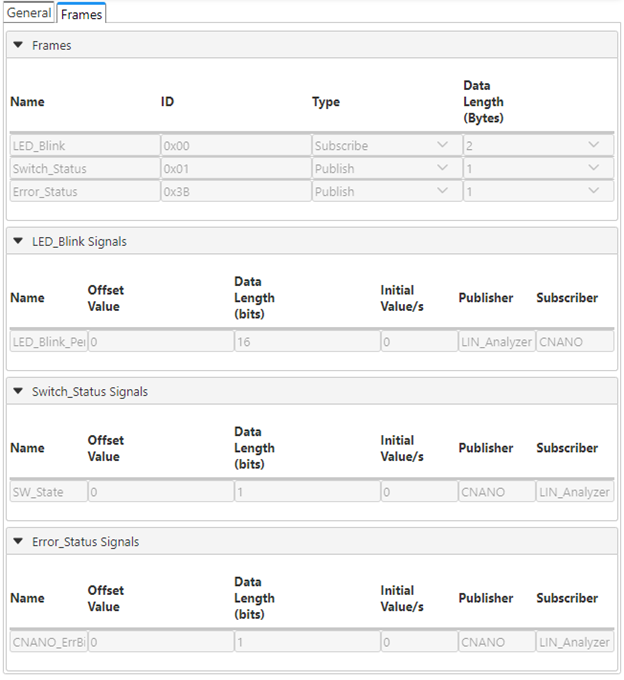
4.4.4 Frame Processor Configuration
In the General tab, configure the Frame Processor mode to “Non-blocking”
Figure 4-7. Frame Processor Configuration 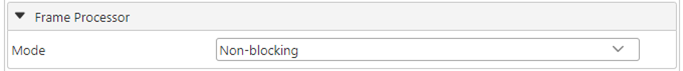
4.4.5 UART and Timer Configuration
- Select EUSART1 as the LIN Responder’s UART and set the baud rate to 19200. The baud rate is already filled in and uneditable when an LDF is loaded.
Select TMR0 as the Timer
Figure 4-8. LIN UART and Timer Configuration 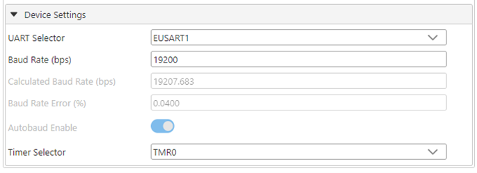
4.4.6 Pins Configuration
Go to the Pin Grid View tab and configure EUSART1 pins: TX1 to RC2 and RX1 to RC3
- Set RD4 and RE0 as GPIO output pins, and RE2 as
an input pin
Figure 4-9. Pin Grid View 
Click the Pins block from the Application Builder. Configure the pins as shown below.
Figure 4-10. Pin Configuration 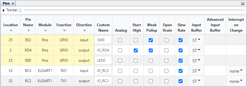
4.4.7 Adding Timer for LED Blink
Add a 16-bit timer to generate an interrupt every 1 ms period. This resource will be used for blinking the CNANO LED and is different from the configured LIN Responder’s timer.
- Load Timer1 from Device Resources
- Under Hardware Settings, enable Timer and 16-Bit Read/Write mode
Set the Requested Period to 1 ms and enable TMR Interrupt
Figure 4-11. LED Blink Timer Configuration 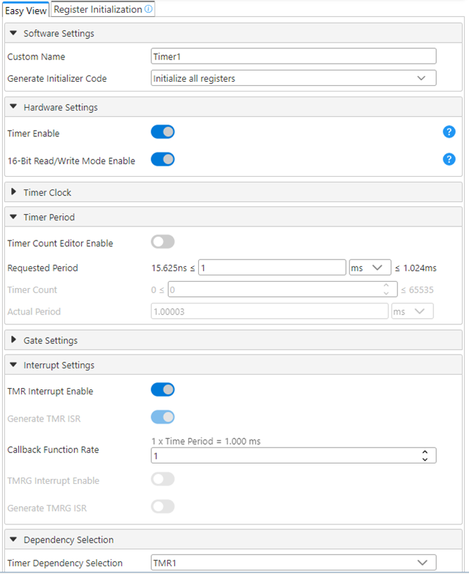
4.4.8 Generating the Code
- Go to the Notifications tab and address any warnings. Take note of the Hints.
- Hit the Generate button next to Project Resources
4.4.9 Adding the Application Code
- After a successful generation, open the
main.cfile and add the following code:#include "mcc_generated_files/system/system.h" /* Main application */ void LED_BlinkPeriodSet(void); void SW_StatusRead(void); void LED_Toggle(void); void Timer_Stop(void); uint16_t blinkPeriod = 0; uint16_t counter = 0; int main(void) { SYSTEM_Initialize(); // Enable the Global Interrupts INTERRUPT_GlobalInterruptEnable(); // Enable the Peripheral Interrupts INTERRUPT_PeripheralInterruptEnable(); LEDBLINK_AppCallbackRegister(LED_BlinkPeriodSet); LINRESP_ShortRespErrCallbackRegister(Timer_Stop); Timer1_OverflowCallbackRegister(LED_Toggle); while (1) { SW_StatusRead(); } } void LED_BlinkPeriodSet(void) { Timer1_Stop(); blinkPeriod = l_u16_rd_LED_Blink_Period(); counter = 0; Timer1_CounterSet(0); Timer1_Start(); } void LED_Toggle(void) { if(++counter == blinkPeriod) { LED0_Toggle(); counter = 0; } } void SW_StatusRead(void) { if (SW0_GetValue() == HIGH) { l_bool_wr_SW_State(0); } else { l_bool_wr_SW_State(1); } } void Timer_Stop(void) { Timer1_Stop(); }
Do a Clean and Build

If there are no build issues, hit Make and Program Device

4.5 LIN Analyzer Setup
- Open the LIN Serial Analyzer software
Go to Tools and Options>Configure LIN Analyzer and set the baud rate to 19200
Figure 4-12. LIN Analyzer Configuration 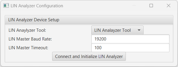
- Hit the Connect and Initialize LIN Analyzer button before closing the pop-up window. A “LIN Analyzer initialized” status is displayed in the footer of the main window.
In the main UI, add the following LIN frames and set the Checksum Type to “Enhanced”
Figure 4-13. LIN Analyzer Frames 
- Select the frames to be sent and click the Send Once button
4.6 Demo Output
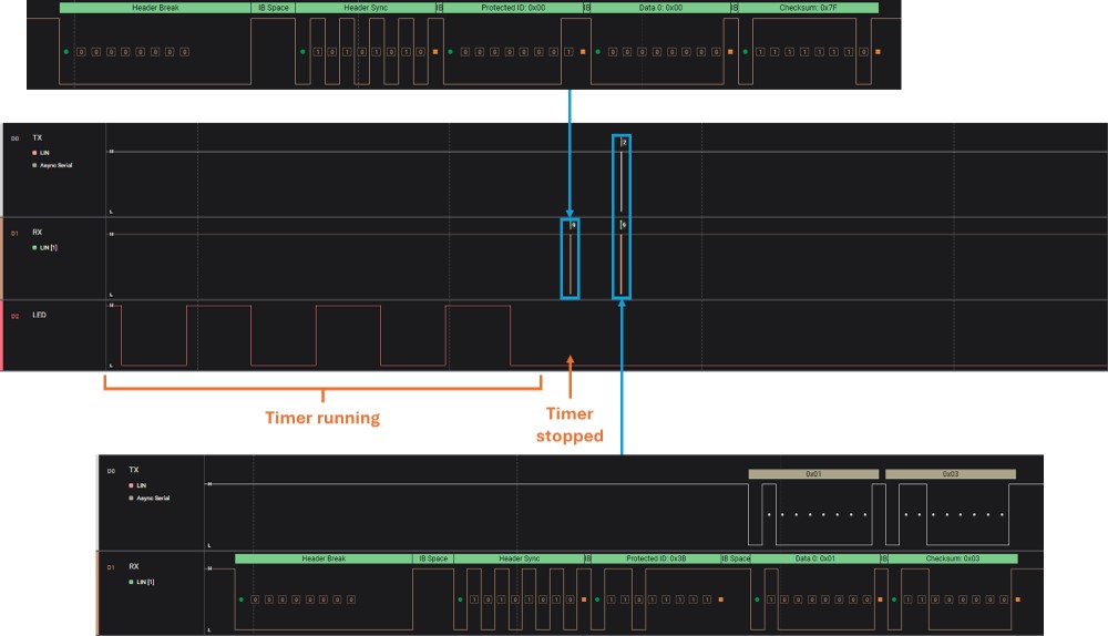
A sample output of the LIN Serial Analyzer is shown below. The LIN Analyzer window displays the Protected Identifier (PID) of each frame on the Frame ID column.

LED Blink Frame (ID = 0x00, PID = 0x80)
Byte 0 and Byte 1 of this frame correspond to the lower and upper byte the LED blink period with a time base of 1 ms.
Changing the data from [FF 00] to [E8 03], which are equivalent to 0x00FF and 0x03E8 in 16-bit hex, respectively, will update the Responder node’s LED blink period from ~255 ms to ~1000 ms. 0x00FF is equivalent to 255 in decimal while 0x03E8 is equal to 1000.

Switch Status Frame (ID = 0x01, PID = 0xC1)
This frame includes a Boolean signal corresponding to the state of the CNANO’s on-board switch.
Bit 0 of the frame’s Byte 0 is set to ‘1’ when the button is pressed
and ‘0’ if released.
Error Status Frame (ID = 0x3B, PID = 0xFB)
This frame includes a Boolean signal for the error bit required for LIN 2.x. Bit 0 of the frame’s
Byte 0 is set to ‘1’ when the previous frame includes an error.
In the above example, a “response too short” error was introduced by sending an incomplete frame with PID 0x80. The Responder node expects two bytes of data and the checksum byte. Since the Commander transmitted only one data byte and the checksum byte within the time-out period, the Responder flagged this frame as erratic and automatically set the error signal bit.
The application program stops the LED blink timer when a Response Too Short error is detected.