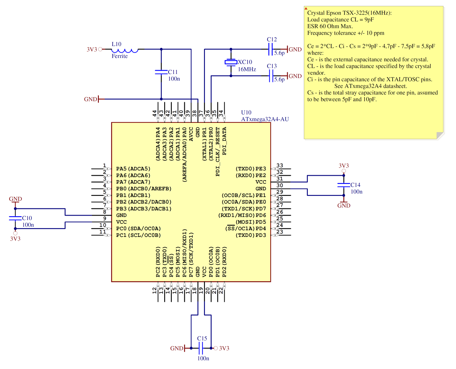
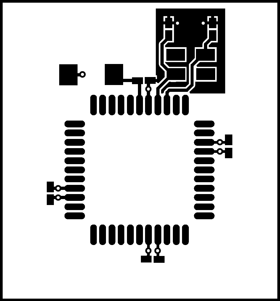
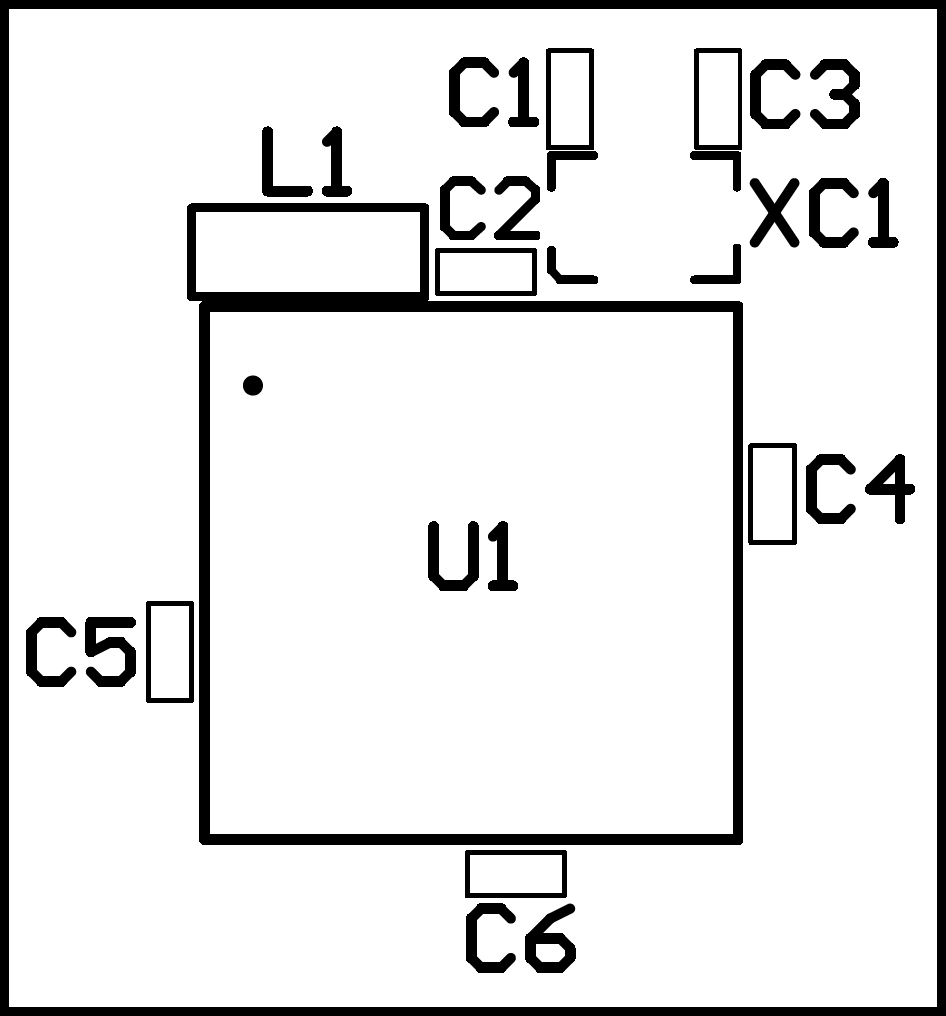
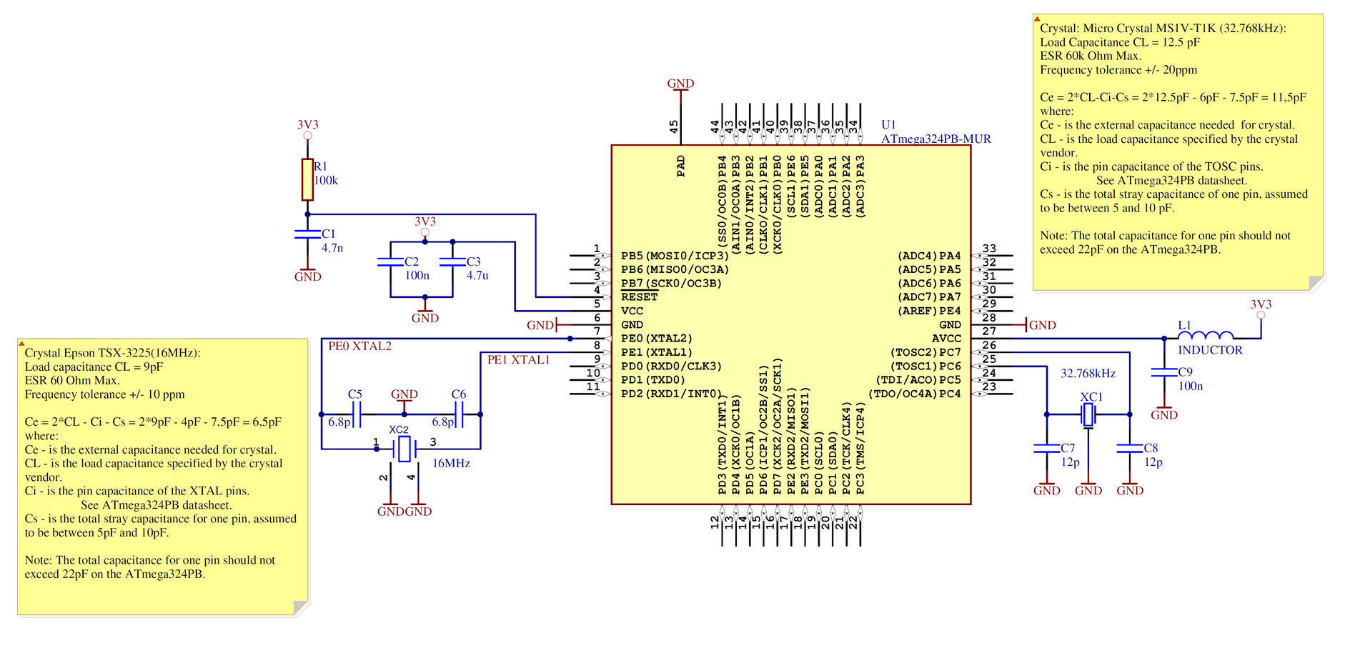
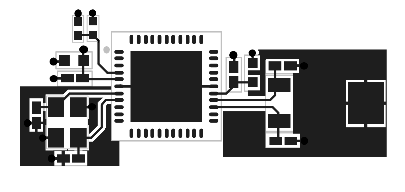
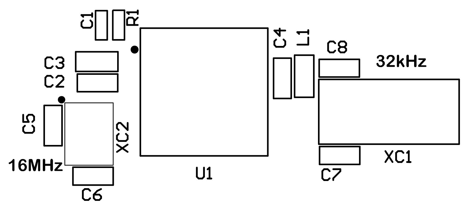
7 Example Layout of ATxmega32A4 and ATmega324PB Devices
The following schematic- and layout examples are recommended starting points
for ATxmega32A and ATmega324PB designs. Always check the respective data sheets to
ensure the correct values are used for all components. The key points to be considered
are:
- The connections for crystal oscillator and decoupling capacitors.
- The number of layers on the PCB. It is recommended to have a multilayer design with supply and ground plane on separate layers.
- Decoupling of all digital supply pairs from VCC and isolating AVCC from VCC.
- Short distance between the crystal/capacitors and the MCU.
- Ground plane surrounding the crystal and the vias connected to the planes are close to the MCU pins in the layout.
Note: For ATmega PB devices, the total amount
of capacitance must not exceed 22 pF. This includes PCN traces and pin
capacitance.
