In order to keep up with the sampling rate and prevent loss of data, two GPR banks are used as ping-pong buffers to write to buffer RAM. A ping-pong buffer is a double-buffer, which increases the throughput of the system by speeding up the read/write process. In the application, GPR banks 11 and 12 are used as ping-pong buffers.
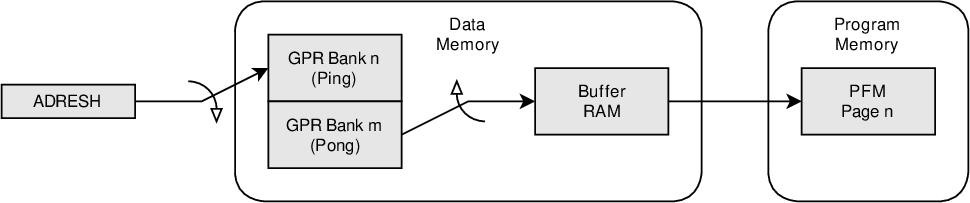
In Figure 2-1, GPR banks n and m are
arranged together as a ping-pong buffer. When the DMA is writing data to GPR Bank n
(ping), another DMA is busy transferring data out of GPR bank m (pong) into the buffer
RAM. The NVMUI then writes the contents of the buffer RAM into the selected PFM page.
See Data Transfer from Ping-Pong Buffers to Internal Memory for details on how to write to
internal memory.
Figure 1. Ping-Pong Buffer Transfer to
Internal Memory
If the data is being transferred to external Flash memory, then another DMA can be
configured to write to the SPI transfer buffer instead. The SPI must be pre-configured
to write to the external memory. See Data Transfer from Ping-Pong Buffers to External Memory for details on how to write to external
memory.
Figure 2. Ping-Pong Buffer Transfer to
External Memory

Tip: It is recommended
for the two GPR banks for ping and pong buffers to reside adjacent to each other in
memory. This allows one single DMA to service the entire ping buffer and pong
buffer spaces, without the need to reconfigure DMA when transitioning between
buffers. If the ping buffer and pong buffer are not adjacent, then the DMA will need
to be reconfigured whenever buffer transition is required.