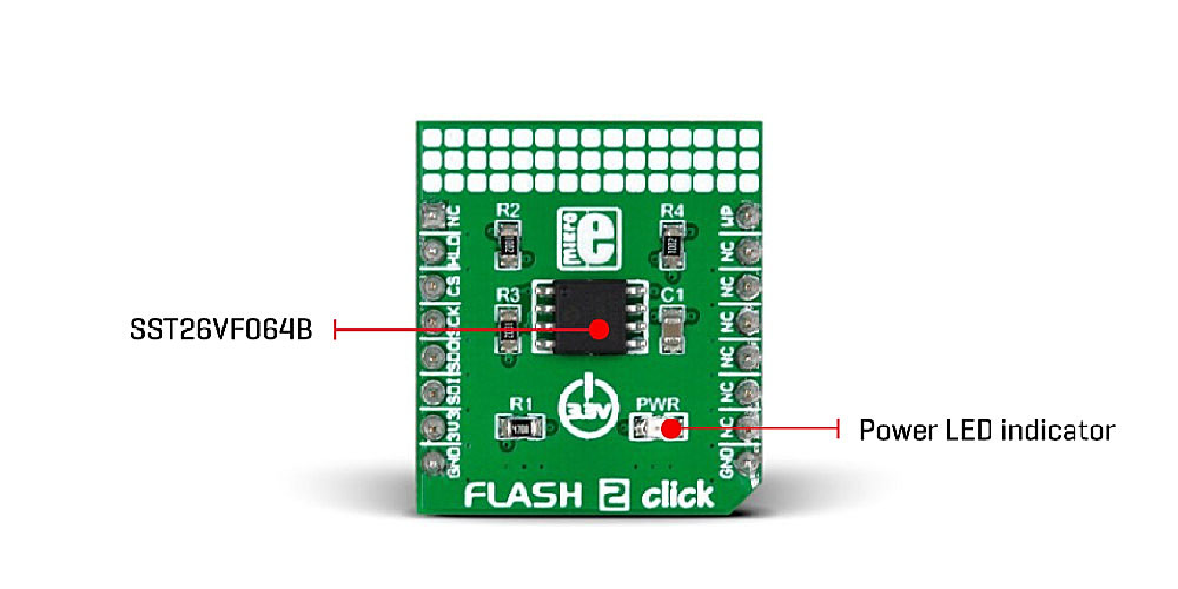
The SST26VF064B can be written one page at a time. The Page
Program instruction allows up to 256 bytes to be written during one write cycle.
Data can be read by the Read Data Bytes instruction. While reading, the
address increment is automatically executed, making it possible to read the entire memory by a
single Read Data command. The Page Program instruction can
only reset the bits to 0. Therefore, a segment of memory needs to be erased prior to
programming or, in this case, filled with 1s (0xFF). The SST26VF064B allows erasing one sector
at a time (Sector Erase instruction), one block at a time (Block
Erase instruction) and the entire memory (using the Chip Erase
instruction).
See Data Transfer from Ping-Pong Buffers to External Memory and Data Transfer from External Memory to DAC for details on how to write to and read from the external memory.