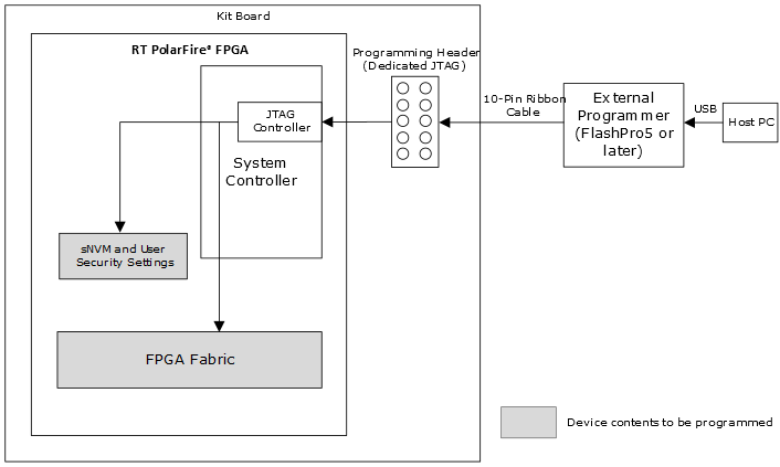
Microchip FlashPro programmer v5 or later can be used to program RT PolarFire FPGA through the dedicated JTAG interface. This can be done either using the Libero SoC or a standalone FlashPro Express.
The FlashPro programmer connects to the device via a 10-pin programming header using a FlashPro cable (10-pin ribbon), as shown in the following figure.
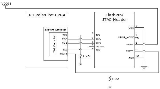
The following table lists the FlashPro header signals.
| Pin Number | Signal | Direction to FlashPro Programmer | Description |
|---|---|---|---|
| 1 | TCK/SCK | Output | JTAG/SPI clock. |
| 2 | GND | — |
Signal reference. GND pins must be connected. |
| 3 | TDO/MISO | Input | JTAG/SPI data output from programming device. |
| 4 | PROG_MODE | Not connected | Unused |
| 5 | TMS/SS | Output | JTAG test-mode select/SPI slave select. |
| 6 | VJTAG/VSPI | — |
Target interface voltage input. |
| 7 | VPUMP | Not connected | Unused |
| 8 | TRSTB | Output | JTAG test reset. |
| 9 | TDI/MOSI | Output | JTAG/SPI data input to programming device. |
| 10 | GND | — |
GND |
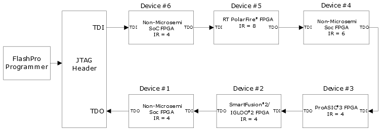
A single FlashPro programmer can program multiple Microchip FPGAs from the same family or from different families in a single JTAG chain. The TDO pin of the JTAG header represents the beginning of the chain. The TDI pin of the last device connects back to the JTAG header, thus completing the JTAG chain. The following types of FPGAs can be added to a JTAG chain:
- Microchip devices targeted for programming
- Microchip bypass devices not targeted for programming
- Non-Microchip bypass devices
When a device is in Bypass mode, the device’s data register length is automatically set to 1 and the device stops responding to any programming instructions. To place a device in bypass mode, the instruction register (IR) length must be known. For Microchip FPGAs, the IR length is obtained automatically by the FlashPro Express. For non-Microchip FPGAs, the boundary scan description language (BSDL) file, which contains a sequence of boundary scan commands and data, must be loaded, or the IR length must be manually entered in the FlashPro Express. For more information about JTAG chain programming, see FlashPro User’s Guide.
For information about power supply requirement and filtering capacitors, see UG0726: PolarFire FPGA Board Design User Guide.
The following figure shows the connections between the programming header and the device.