The following figure illustrates the IO Port Configuration within the IO Ports tab for setup of the IO port pins of the ATA8510 device at start-up time. These settings change when executing the ROM firmware or Flash application. For more details on the EEPROM port pin configuration, refer to the ATA8510/15 Industrial User's Guide (DS50003142). For more details about debug support, refer to the ATAN0096 ATA8510 Programmer's Guide.
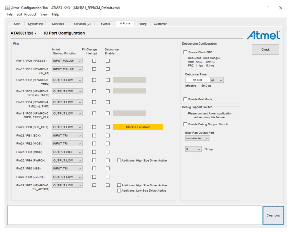
The preceding figure illustrates the default settings that define the IO pin configurations. To select and enable the alternative functions in other tabs, see the following table for port B, and Table 2 for port C. Enable these alternative settings within the ROM firmware or the Flash application and overwrite the initial settings from the IO ports configuration. For more details about the IO ports and the alternate functions, refer to the ATA8510/15 Industrial User's Guide (DS50003142).
|
Pin |
Alternate Function |
Activation in Tab |
GUI Function |
|---|---|---|---|
|
“PB0” |
“CLK_OUT” |
System Init – Clock |
Check Clock Output Enable |
|
“PB1” |
“SCK” |
— |
Always SPI clock input |
|
“PB2” |
“MOSI” |
— |
Always SPI data input |
|
“PB3” |
“MISO” |
— |
Always SPI data output |
|
“PB4” |
“PWRON” |
— |
Active during power-up |
|
“PB5” |
“NSS” |
— |
Always SPI peripheral select input |
|
“PB6” |
“EVENT” |
— |
Always event output |
|
“PB7” |
“NPWRON6” |
— |
Active during power-up |
|
“RX_ACTIVE” |
System Init – RX Active Pin (PB7) |
Check RX Active Enable |
| Pin | Alternate Function | Activation in Tab | GUI Function or Comment |
|---|---|---|---|
| “PC0” | “NRESET” |
— |
The fuse setting enables the device reset |
| “CSC0” | Services (2) – Channel Switch Control |
Enable channel 0 switch output (only use when reset is disabled) |
|
| “PC1” | “NPWRON1” |
— |
Active during power-up |
| “CSC1” | Services (2) – Channel Switch Control | Enable channel 1 switch output | |
| “LIN_EN” |
— |
Enable signal for LIN transceiver (LIN implemented by software) |
|
| “PC2” | “NPWRON2” |
— |
Active during power-up |
| “TRPA” | Services – Path A, Demodulation Settings | Raw Transp. Output | |
| “CSC2” | Services (2) – Channel Switch Control | Enable channel 2 switch output | |
| “PC3” | “NPWRON3” | Active during power-up | |
| “TMDO” | Services – RF Settings | Reshaped Transp. Output | |
| “TxD(Lin)” |
— |
Connected to timer4 TM1 output signal (LIN implemented by software) |
|
| “CSC3” | Services (2) – Channel Switch Control | Enable channel 3 switch output | |
| “PC4” | “NPWRON4” |
— |
Active during power-up |
| “TMDI” |
— |
Selected with transparent TXMode (must set to input) |
|
| “RxD(Lin)” |
— |
Connected to timer4 TICP input signal (LIN implemented by software) |
|
| “CSC4” | Services (2) – Channel Switch Control | Enable channel 4 switch output | |
| “PC5” | “NPWRON5” |
— |
Active during power-up |
| “TRPB” | Services – Path B, Demodulation Settings | Raw Transp. Output | |
| “TMDO_CLK” | Services – RF Settings | Reshaped Transp. Output | |
| “CSC5” | Services (2) – Channel Switch Control | Enable channel 5 switch output |