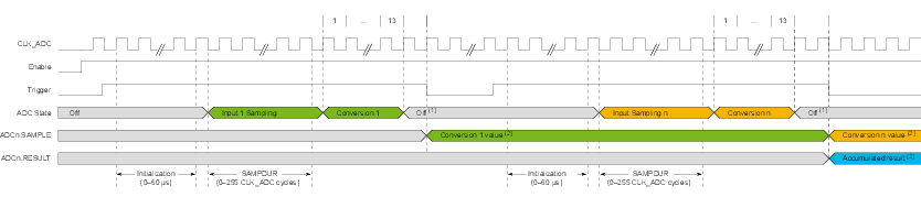
The figure below shows the timing diagram for the ADC when running in Series Accumulation mode without using the PGA.
Figure 1. Timing Diagram - Series
Accumulation
Notes:
- 1.If the Low Latency (LOWLAT) bit is set to ‘
1’ in the Control A (ADCn.CTRLA) register, the analog modules in the ADC will not turn OFF at the end of the conversion, eliminating the initialization time when triggering the following conversion. - 2.The time from the conversion has finished to the outputs are available in the registers is 0.5 CLK_ADC cycles followed by 1 CLK_MAIN cycle. The last conversion and accumulation require an additional CLK_MAIN cycle. With minimum prescaling, this sums up to 1.5 CLK_ADC cycles before the final outputs are available.
The number of samples to accumulate is set by the Sample Number (SAMPNUM) bit field in the Control F (ADCn.CTRLF) register.
The total conversion (tsamp) time for each separate sample, in μs, is calculated by: