| Symbol | Pins | I/O | Description |
|---|---|---|---|
| MOSI | PB5 | I | Serial Data in |
| MISO | PB6 | O | Serial Data out |
| SCK | PB7 | I | Serial Clock |
Figure 1. Serial Programming and
Verify(1)
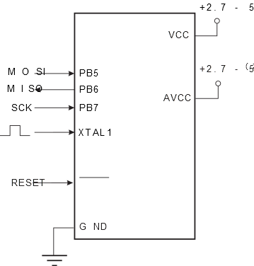
Notes:
- 1.If the device is clocked by the Internal Oscillator, it is no need to connect a clock source to the XTAL1 pin.
- 2. VCC - 0.3 < AVCC < VCC + 0.3, however, AVCC should always be within 2.7 - 5.5V.
When programming the EEPROM, an auto-erase cycle is built into the self-timed programming operation (in the Serial mode ONLY) and there is no need to first execute the Chip Erase instruction. The Chip Erase operation turns the content of every memory location in both the Program and EEPROM arrays into 0xFF.
Depending on CKSEL Fuses, a valid clock must be present. The minimum low and high periods for the Serial Clock (SCK) input are defined as follows:
Low: > 2 CPU clock cycles for fck < 12MHz, 3 CPU clock cycles for fck ≥ 12MHz
High: > 2 CPU clock cycles for fck < 12MHz, 3 CPU clock cycles for fck ≥ 12MHz