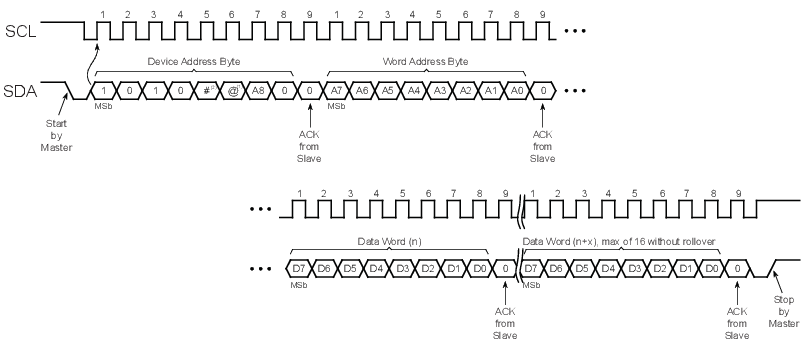
A page write operation allows up to 16 bytes to be written in the same write cycle, provided all bytes are in the same row of the memory array (where address bits A9/A8 to A3 are the same). Partial page writes of less than 16 bytes are also allowed.
A page write is initiated the same way as a byte write, but the bus master does not send a Stop condition after the first data word is clocked in. Instead, after the EEPROM acknowledges receipt of the first data word, the bus master can transmit up to fifteen additional data words. The EEPROM will respond with an ACK after each data word is received. Once all data to be written has been sent to the device, the bus master must issue a Stop condition (see Figure 1) at which time the internally self-timed write cycle will begin.
The lower four bits of the word address are internally incremented following the receipt of each data word. The higher order address bits are not incremented and retain the memory page row location. Page write operations are limited to writing bytes within a single physical page, regardless of the number of bytes actually being written. When the incremented word address reaches the page boundary, the address counter will rollover to the beginning of the same page. Nevertheless, creating a rollover event should be avoided as previously loaded data in the page could become unintentionally altered.