3 Free-Running to External I/O
This example shows a basic initialization and link to I/O ports of the ZCD peripheral. This example is used to obtain PWM representation of a sinusoidal AC signal, and the ZCD is working independently of the CPU.
How to select the external components
The AC signal was obtained from the signal generation capability of the oscilloscope. It has a sinusoidal 5V peak-to-peak amplitude and is offset by one volt from ground to compensate for ZCPINV. Using Equation 2-1, the selected RSERIES value is approximately 10 kΩ. The connection setup is depicted in Figure 3-2.
How to set up the internal circuit
- Configure the desired input
pin in the PORT peripheral as an analog pin with digital input buffer
disabled.
Internal pull-up and pull-down resistors must also be disabled.
To allow the zero-cross detection, the ZCD input has to be connected to the sensing voltage using an I/O pin. This pin needs to have the digital input buffer and the pull-up resistor disabled, to have the highest possible input impedance. For the AVR128DA48, PORTD pin 1 (PD1) is used as ZCD0 negative input, as depicted in the figure below.
Figure 3-1. ZCD I/O Connections This translates to the following code:
PORTD.PIN1CTRL |= PORT_ISC_INPUT_DISABLE_gc;
- Optional: Enable the output
pin by writing a ‘
1’ to the Output Enable (OUTEN) bit in the Control A (ZCDn.CTRLA) register and set the desired pin as an output.For the AVR128DA48, PORTA pin 7 (PA7) is used as ZCD0 output, as depicted in the figure above.
This translates to the following code:
ZCD0.CTRLA = ZCD_OUTEN_bm;
PORTA.DIRSET |= PIN7_bm;
PORTA.OUTSET |= PIN7_bm;
- Enable the ZCD by writing a
‘
1’ to the ENABLE bit in ZCDn.CTRLA.After the ZCD is enabled, there is a start-up time during which the output of the ZCD may be invalid. Refer to the Electrical Characteristics section in the device data sheet for the typical value of the start-up time.
Enabling the ZCD can be done using the following line of code:
ZCD0.CTRLA = ZCD_ENABLE_bm;
All this can be encapsulated into one initialization function (e.g., ‘
ZCD_Init’) to keep the code easier to follow.
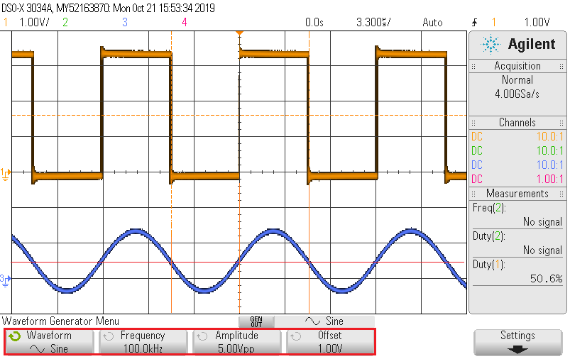
The oscilloscope measurements from Figure 3-3 depicts the input and output of the ZCD as it works in Free-Running mode measured from the I/O pins of the MCU.

The STATE bit in the ZCDn.STATUS register indicates whether the input signal
is above or below the reference voltage, ZCPINV. By default, the STATE bit is
‘1’ when the input signal is above the reference voltage and
‘0’ when the input signal is below the reference voltage. The
polarity of the STATE bit can be reversed by writing the INVERT bit to
‘1’ in the ZCDn.CTRLA register. The INVERT bit will also affect the
ZCD interrupt polarity.