
3.4.2 Implementation Example for DDR3L
When routing a 16-bit bus width DRAM interface, it is recommended to use 16-bit memory devices. The single memory device should be routed in a simple point-to-point topology.
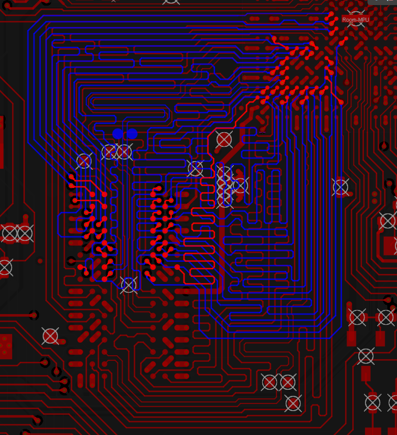
Traces belonging to the address, command and control group should be length-matched within this group.
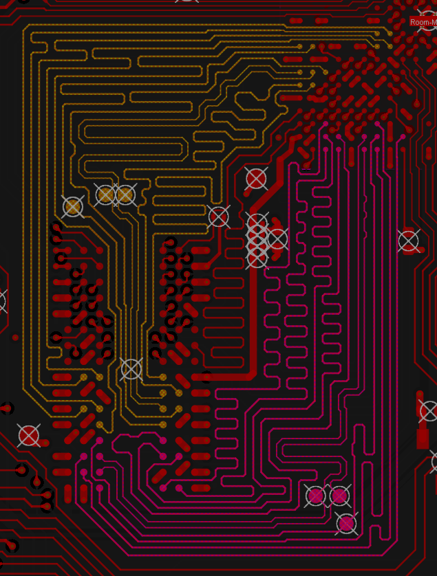
Traces from each data byte lane should also be matched within its own lane.
It is also good practice to route data signals that belong to the same byte lane on the same layer. Figure 3-10 shows the signal routing of data byte lanes 0 and 1. For the address/command/control signals bus in Figure 3-9, the routing constraints can be more relaxed and the routing can be made on any available signal layer.
It is recommended to route the DRAM clock and DQS differential signals on the top and bottom layers, or on the same layer as the other signals from the same group.
When routing the MIPI signals, a maximum of 0.15 mm length mismatch is allowed within the differential pair and a maximum of 1.5 mm length mismatch is allowed between differential pairs.
It is recommended to match any group of high-speed signals as tightly as possible.