7 Getting Started with GPIO
7.1 Introduction
| Authors: Alexandru Niculae, Catalin Visan, Microchip Technology Inc. |
The purpose of this document is to describe step-by-step how to use the microcontroller’s pins as General Purpose Input/Output (GPIO) on Microchip tinyAVR® 0- and 1-series, megaAVR® 0-series and AVR® DA devices. The following use cases are presented:
- Blink an
LED:
Blink an LED using a delay, toggling the LED every 500 ms.
- Long and
Short Button Press:
Use a pin as input to distinguish between a long and short button press, defined by a delay threshold. An LED will toggle every 100 ms if a long press is detected, and every 500 ms if a short press is detected.
- Wake-Up On
Button Press:
Exit sleep on button press, turn on an LED, and go back to sleep. On button release - exit sleep, turn off the LED, and go back to sleep.


7.2 Overview
The instances of the PORT peripheral registers control the I/O pins of the device. Each port instance has up to eight I/O pins. The ports are named PORTA, PORTB, PORTC, etc. All pin functions are configurable individually per pin.
For best power consumption, disable the input of unused pins, pins used as analog input, and pins used as outputs.
Specific pins, such as those used for connecting a debugger, may be configured differently, as required by their special function.

7.3 Blink an LED
This section demonstrates how to turn an LED on and off alternatively.
Although this use case is very simple, it is widely used in real life applications, and it helps in understanding how to achieve some of the very basic functions of the microcontroller. These functions are:
- Setting a pin direction
- Setting the output value of a pin
Setting a Pin Direction
The directions of the pins are stored in the PORTn.DIR register. For example, the
directions for the pins of PORTA are stored in PORTA.DIR. Each bit in the register
controls the direction of the corresponding pin, so PORTA.DIR bit 0 controls pin A0
(also called PA0). For a bit value of ‘1’, the pin is configured as
output, while for ‘0’, it is configured as input.
In most cases, it is only necessary to write one bit at a time. For this purpose,
there are eight bitmasks (PINx_bm) defined in the <avr/io.h>
header file, one for each bit. These macros represent bitmasks that have a
‘1’ bit on x position and ‘0’ bits in rest.
For example, PIN5_bm is 0b00100000. Using these bitmasks in
conjunction with logic operations makes it possible to only write the corresponding
pin and make sure the others are unchanged.

To set (write to ‘1’) pin x, use:
PORTn.DIR = PORTn.DIR | PINx_bm;
This because a logic OR operation with ‘1’ will
always result in ‘1’, while logic OR with
‘0’ will leave the value unchanged (1|1 = 1, 1|0 = 1, 0|0 = 0).
Hence, the bitmask only has ‘1’ on the position to be set.
To clear (write to ‘0’) pin x, use:
PORTn.DIR = PORTn.DIR & ~PINx_bm;
This because a logic AND operation with ‘0’ will
always result in a ‘0’, while logic AND operation
with ‘1’ will leave the value unchanged (1&1 = 1, 1&0 = 0,
0&0 = 0). Hence, the bitmask only has ‘0’ on the position to
clear.
- The same approach, to only modify a single bit, can be used for all other registers as described in previous paragraphs.
- Logic operations with more bitmasks can be chained in an expression such as PORTA.DIR = PORTA.DIR | PIN0_bm | PIN1_bm.
- PINx_bp are similar macros that define the position of the bit in the register. For example, PIN2_bp has the value 2. The bitmask macros can be obtained using these macros and the shift operation.
Setting the Output Value of a Pin
The PORTn.OUT register controls the output values, so that ‘0’ means
the pin will be pulled to GND and ‘1’ means it will be pulled to
VDD.
0’ and ‘1’, can be inverted using the
PORTn.PINxCTRL register. See the PORTn.PINxCTRL register section in the data sheet
to understand its functionality.
As previously described, the same approach to only modify a single bit can be applied to write to the PORTn.OUT register.
The following code toggles pin PB5 each 500 ms. An LED is attached to that pin on the ATmega 4809 Xplained Pro board.
#define F_CPU 3333333
#include <avr/io.h>
#include <avr/delay.h>

int main(void)
{

    PORTB.DIR |= PIN5_bm;

    while (1)
    {
 		PORTB.OUT |= PIN5_bm;
 		_delay_ms(500);
         PORTB.OUT &= ~PIN5_bm;
 		_delay_ms(500);
    }
}
- To use the delay functions,
F_CPU must be defined before including
avr/delay.h. F_CPU must match the CPU frequency. - The PORTn.OUTTGL register can also be used to toggle a pin.
- As an optimization, PORTn.OUTSET/PORTn.OUTCLR and PORTn.DIRSET/PORTn.DIRCLR registers can also be used to set the pin direction and output value. Their benefit is that instead of the read-modify-write operation, only a write operation is used.

An MCC generated code example for AVR128DA48 with the same functionality as the one described in this section can be found here:

7.4 Long and Short Button Press
This section explains how to detect whether a button press is long or short, resulting in two different scenarios.
The GPIO interface can be used to sense external digital signals in order to make certain decisions. In this regard, the application range is vast, so the AVR controllers can be configured several of ways to match as many use cases as the user might need. In this section, the focus will be on the push of a button.
First, PB2 will be configured as input by writing a ‘1’ on
bit 2 of the Data Direction Clear (PORTB.DIRCLR) register.

PORTB.DIRCLR = PIN2_bm;
For a button connected between the GPIO pin and GND to work correctly, connect a pull-up
resistor between the GPIO pin and VDD. This configuration will make sure the
pin reads a default value of logic ‘1’ when the button is not pressed.
It is possible to activate an internal pull-up resistor from the Pin 2 Control
(PORTB.PIN2CTRL) register.

PORTB.PIN2CTRL = PORT_PULLUPEN_bm;
For a better user experience, an LED-connected PB5 will blink with different frequency
based on the type of press. Thus, PB5 will be configured as output by writing a
‘1’ on bit 5 of the Data Direction Set (PORTB.DIRSET) register.
PORTB.DIRSET = PIN5_bm;
Then, in each iteration of the main loop, bit 2 of the Input Value
(PORTB.IN) register will be checked. If the value is logic ‘0’, the
program will wait until the value is back to logic ‘1’. By doing this,
the program will sense when a press-and-release action on the button was performed.
While waiting, a counter will be incremented every few milliseconds.
If the value of the counter passes a certain threshold, the program will decide there was a long press. If the button is released before passing the threshold, the program will decide there was a short press. Depending on the press type, the LED will blink with different frequencies.

if(~PORTB.IN & PIN2_bm) /* check if PB2 is pulled to GND */
    {
        while(~PORTB.IN & PIN2_bm) /* wait until PB2 is pulled to VDD */
        {
            _delay_ms(STEP_DELAY);
            counter++;
            if(counter >= THRESHOLD)
            {
                LED_blink(LONG_DELAY);
                while (~PORTB.IN & PIN2_bm) /* wait until PB2 is pulled to VDD */
                }
                    ;
                }
                break;
            }
        }
        if(counter < THRESHOLD)
        {
            LED_blink(SHORT_DELAY);
        }
        counter = 0;
}
<util/delay.h> header file.The LED_blink function takes the blinking period in milliseconds divided by two as a
parameter. The function must be declared “inline” because the _delay_ms
macro must take a parameter that is already known at the compilation stage.
inline void LED_blink(uint32_t time_ms)
{
        for(uint8_t i = 0; i < NUMBER_OF_BLINKS ; i++)
        {
            PORTB.OUT |= PIN5_bm;
            _delay_ms(time_ms);
            PORTB.OUT &= ~PIN5_bm;
            _delay_ms(time_ms);
        }
}
An MCC generated code example for AVR128DA48 with the same functionality as the one described in this section can be found here:
7.5 Wake-Up On Button Press
This example demonstrates the usage of interrupts and sleep modes. In this use case, the microcontroller exits sleep on button press, turns on an LED, and goes back to sleep. On button release, it exits sleep, turns off the LED, and goes back to sleep. The LED is ON while the button is pressed, but the microcontroller can be in sleep mode.
Pins can detect transitions from ‘0’ to ‘1’ (rising
edge) and from ‘1’ to ‘0’ (falling edge). An interrupt
can be triggered on one or both transitions. This is configured using the ISC bit field
in the PORTx.PINnCTRL register.

These interrupts wake the device from all sleep modes. In this example, on button press/release, the microcontroller will wake from sleep and turn an LED on/off and then go back to sleep. In this way, the LED will stay on only while the button is pressed.
First, the B2 pin, where the button is attached, is configured as input, and its interrupt is activated.
PORTB.DIR &= ~ PIN2_bm;
PORTB.PIN2CTRL |= PORT_PULLUPEN_bm | PORT_ISC_BOTHEDGES_gc;
0’. Therefore, whenever the
button is not pressed, it must be connected to VDD using a pull-up resistor.
The pull-up resistor is activated using the PULLUPEN bit field in the PORTx.PINnCTRL
register.Second, the sleep mode is selected using the macros defined in the
<avr/sleep.h> header. The modes of sleep are Idle, Standby
and Power-Down. In this example, the deepest sleep mode is used.
set_sleep_mode(sleep_MODE_PWR_DOWN);
This only selects which sleep mode to be used. The following macro makes the microcontroller go to sleep.
sleep_mode();
sleep_mode() macro
also enables sleep before sending the CPU sleep instruction and
disables sleep when the microcontroller wakes up.When going to sleep, the global interrupts must be enabled. Otherwise, there is no way to
wake up. Using the sei() macro defined in the
<avr/interrupt.h> header enables global interrupts. In this
example, this is done in the initialization code.
Sometimes, there are blocks of instructions that need to execute without
interruption. They are called atomic blocks. This is achieved by disabling interrupts at
the beginning of the block and re-enabling them at the end of the block. For this, the
ATOMIC_BLOCK macro in <avr/atomic.h> is
used.
Finally, inside the Interrupt Service Routine (ISR), a flag is set to indicate a transition (rising or falling edge) happened. Because it is a good practice to keep the ISR short, the transition type check and LED toggling are handled in the main-line code.
ISR(PORTB_PORT_vect)
{
    if(PB2_INTERRUPT)
    {
        pb2Ioc = 1;
        PB2_CLEAR_INTERRUPT_FLAG;
    }
}
Because the same interrupt is used for all the pins in a port, the ISR code must check what pin triggered the interrupt. This is done by checking its flag in PORTx.INTFLAGS. In this example, to check whether the pin B2 triggered the interrupt, the following macro is used.
#define PB2_INTERRUPT PORTB.INTFLAGS & PIN2_bm
Clearing the interrupt flag is done by writing a ‘1’ to its
location in PORTn.INTFLAGS.
#define PB2_CLEAR_INTERRUPT_FLAG PORTB.INTFLAGS &= PIN2_bm
The main-line code checks the pin value ten milliseconds after the interrupt
to decide whether it was a falling edge or a rising edge. If the pin is low (value
‘0’), then it must have been a falling edge, otherwise it was a
rising edge. The ten milliseconds delay is a denouncing method.
#define PB2_LOW !(PORTB.IN & PIN2_bm)
An MCC generated code example for AVR128DA48 with the same functionality as the one described in this section can be found here:
7.6 Using GPIO within MCC
The MCC is a user-friendly plug-in tool for MPLAB X and MPLAB Xpress IDEs, which generate drivers for controlling and driving peripherals of PIC® and AVR microcontrollers, based on the settings and selections made in the Graphical User Interface. The generated drivers can be used in any application program.
- For more details about MCC, see the MCC User’s Guide.
- MPLAB Xpress is an online IDE that can be used in the browser.
In MCC, the GPIO pins can be configured in the Pin Manager: Grid View window.

Clicking one of the locks will select the corresponding pin as either input or output, depending on the row clicked. A pin cannot act as input and output at the same time. If the run-time switch between the input and the output is needed, this will have to be manually implemented.
Once selected, the pins will also appear in the Pin Module window.
Various options can be configured here, most of which have already been discussed in this document. If the Output check box is unchecked, the pin will be input.
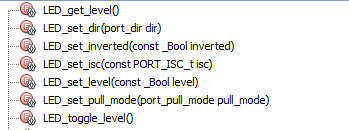
MCC generates macros for the pin usage. The prefix of the macros is the pin name, given in the Custom Name field, which is a helpful abstraction if, for example, one pin controls an LED and its macros can be prefixed with LED instead of the actual pin name.