1.3.2 Live Update Memory Layout for Cortex-M Based
MCUs
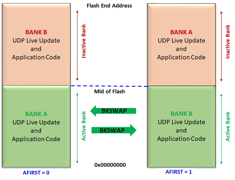
Supported for the devices which have a Dual Bank Flash memory
Internal Flash memory is split into two equal banks. Special NVM Fuse setting
(AFIRST) is used to identify which bank is mapped to NVM main address space after reset.
Start address of Active Bank is always start of Internal Flash memory
Start address of Inactive Bank is from mid of the Internal Flash memory which can vary
from device to device. Refer to the respective Data Sheets for details of Flash memory
layout.
Live Update application start address should always be (0x00000000 to Mid of
Flash). Size of the application should not exceed the Mid of Flash.