
11.1.1 MCC Configuration
The following peripherals need to be configured for realizing the three-phase phase sequence detection demo:
- Timer2 (TMR2)
- Timer4 (TMR4)
- UART1
- SPI1
- ZCD1
- ZCD2
- ADCC
- Pin Module
- Timer2:
Timer2 is configured for 20 ms with the MFINTOSC_500kHz (prescaler 1:64) as the clock source. It is used for scheduling time for executing the phase sequence detection. Figure 11-1 shows the Timer2 configuration window.
Figure 11-1. Timer2 Configuration Window 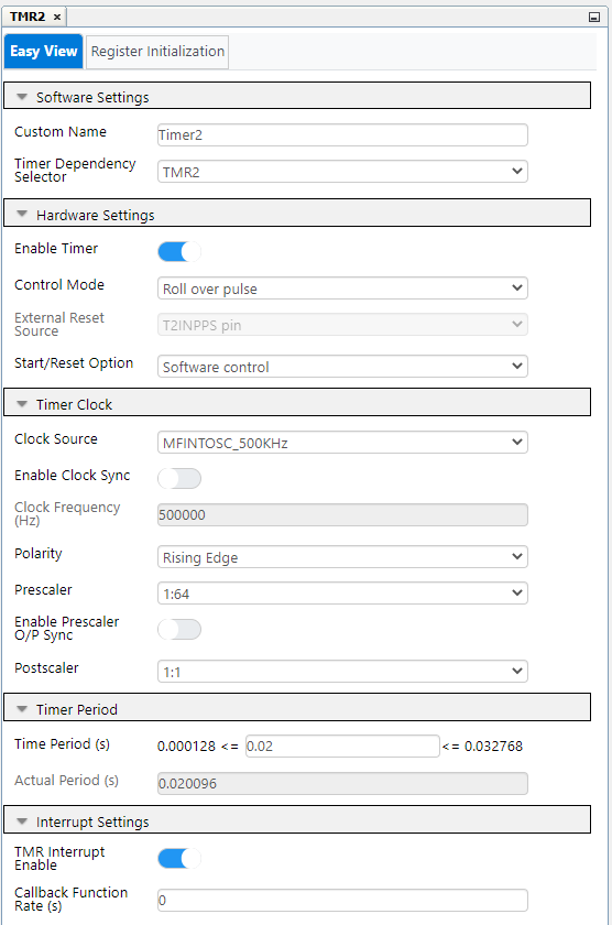
- Timer4:
Timer4 is configured for 1 ms with the system clock divided by 4 (prescaler 1:64) as the clock source. It is used for calculating the phase shift between the two signals out of the three-phase input. Figure 11-2 shows the Timer4 configuration window.
Figure 11-2. Timer4 Configuration Window 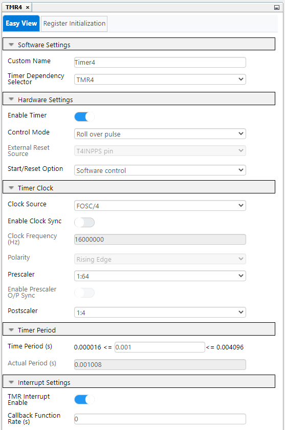
- UART2:
UART2 is configured with a 230400 baud rate, interrupt enabled, and it is used for communication between the application and Data Visualizer. Figure 11-3 shows the UART2 configuration window.
Figure 11-3. UART2 Configuration Window 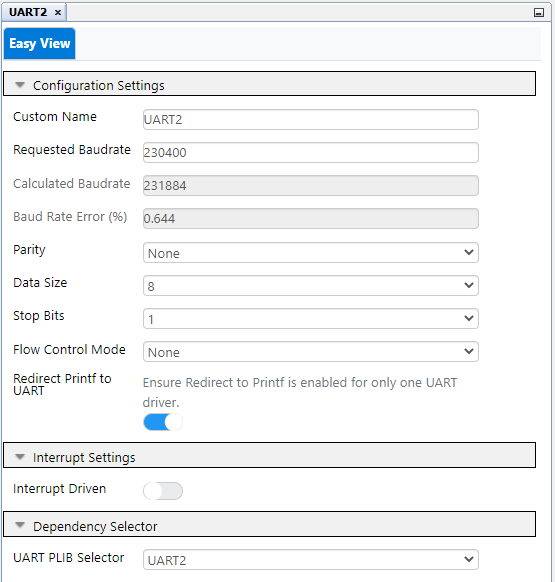
- SPI1:
SPI1 is configured with a 6 MHz speed in mode 2 and it is used for interfacing with the signal emulator modules. Figure 11-4 shows the SPI1 configuration window.
Figure 11-4. SPI1 Configuration Window 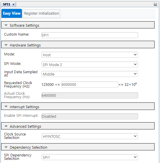
- ZCD1:
ZCD1 is configured with the rising edge detection interrupt enable and it is used for detecting the phase of the three-phase signal. Figure 11-5 shows the ZCD1 configuration window.
Figure 11-5. ZCD1 Configuration Window 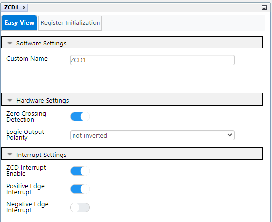
- ZCD2:
ZCD2 is configured with the rising edge detection interrupt enable and it is used for detecting the phase of the three-phase signal. Figure 11-6 shows the ZCD2 configuration window.
Figure 11-6. ZCD2 Configuration Window 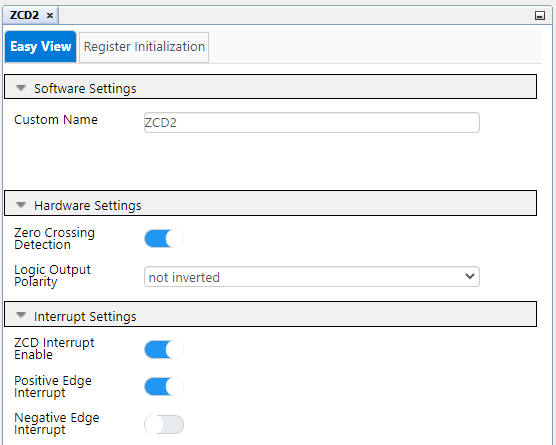
- ADCC:
ADCC is configured in Polling mode and it is used for measuring the three-phase signal to reproduce the signal on the Data Visualizer, calculating the RMS voltage and the single-phasing detection. shows the ADCC configuration window.
Figure 11-7. ADCC Configuration Window 
Pin Module:
Figure 11-8. Pin Module Configuration Window 
Figure 11-9. Pin Module Grid Window 