3.2 Example Systems
An example system-level block diagram for the LAN8679 is shown in Figure 3-2. The VCC pin supplies 3.3V power to the analog transceiver while the VIO pin provides 2.5V or 3.3V power to the TX, RX, and ED I/O. This system does not use sleep mode. In this case, both VIO and VCC are shown connected to the same 3.3V power supply. The TX, RX and ED pins contain an internal pull-up resistor to the VIO supply.
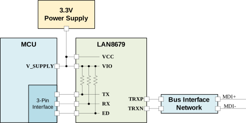
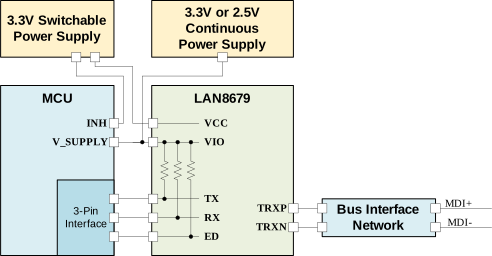
Figure 3-3 shows a system which is designed to use the low-power sleep mode. In this particular system, the external MCU is connected to a switchable 3.3V power supply via an inhibit (INH) pin allowing the MCU to disable the power supply. The switchable supply is connected to the VCC transceiver supply of the LAN8679. In this system, the TX, RX and ED pins are connected to the VIO voltage via internal pull-up resistors. While in sleep mode, the pull-up resistor will pull the TX line high. To exit the sleep state, the MCU digital PHY controller signals a wake event by driving TX low. Alternatively, a wake may be signaled from the network which will cause the transceiver to drive the RX pin low and waking the MCU. Upon wake, the VCC voltage should then be reactivated allowing the LAN8679 to fully power up.