
5.1 OPEN Alliance 3-Pin PMA/PMD Interface
The 3‑Pin PMA/PMD interface is a standardized interface that links the digital PHY consisting of the 10BASE‑T1S PCS and PMA in a microcontroller to an external PMD transceiver. It is defined by the TC14 OPEN Alliance 10BASE‑T1S PMD Transceiver Interface specification. It consists of three pins: TX, RX and ED. The interface is used by the digital PHY controller to configure the transceiver, wake the transceiver, and transfer data to and from the TRXP/TRXN 10BASE‑T1S Ethernet bus. The three pins are used to fulfill different functions depending on which mode the digital PHY controller and transceiver are in.
The TX pin is used to enter and change the different modes of operation. Pulses of different duration and pattern are generated by the digital PHY controller to signal the transceiver to switch into a specific mode. While in the TRANSMITTING state, the polarity of the differential voltage driven on the TRXP/TRXN pair is changed on every falling edge of the TX pin following a Return-to-Zero, Inverted (RZI) encoding scheme. Each low pulse of the TX pin is typically 20 ns. The time the TX pin is high between low pulses is dependent upon the Differential Manchester Encoding (DME) of the data that is performed by the PMA in the microcontroller digital PHY.
While in the NORMAL and TRANSMITTING states, the RX pin is driven low for at least 12 ns each time a change in the differential voltage is detected on the TRXP/TRXN. This allows the digital PHY to receive the same signal pattern on the RX pin that it is sending onto the Ethernet bus via the TX pin. The ED pin is used to indicate whether the differential voltage on TRXP/TRXN is within acceptable bounds, indicating if a valid signal is detected. During the NORMAL state, the digital PHY connected to the microcontroller uses the RX and ED pins to decode the Differential Manchester encoded data on TRXP/TRXN and to detect activity on the line interface. When the device is in TRANSMITTING state and transmitting data onto TRXP/TRXN, the ED pin is used to indicate whether a collision is detected.
In the CONFIGURATION state, the digital PHY controller uses the RX and ED pins to configure the device. In this mode, the RX becomes an MDC pin and the ED pin acts as an MDIO pin. During low power mode, the RX pin is used to distinguish between the low power and low power wake states. The ED pin is used to signal the transceiver status to the digital PHY controller.
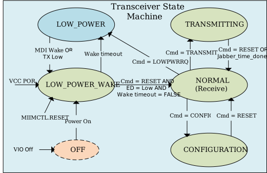
Function States
The digital PHY controller uses the TX pin to send commands and activate the different function states of the transceiver. These states are shown in Figure 5-1 and include the TRANSMITTING, NORMAL, LOW_POWER_WAKE, LOW_POWER, and CONFIGURATION states. Instead of using a data line with a clock to transmit data and activate the functions in the transceiver, the TX pin instead sends pulses of defined length to activate the various states. This is done to reduce electromagnetic emissions.
TRANSMITTING State
In TRANSMITTING state, the digital PHY controller may send data over the TX pin to the transceiver. The transceiver then transmits it onto the Ethernet bus via the TRXP/TRXN pins. The TRXP/TRXN pins are returned to high-impedance when a subsequent RESET Command is sent by the digital PHY controller or when the jabber time expires.
NORMAL (Receive) State
The digital PHY controller may activate the NORMAL state at any time to realign the state machines of the controller and the transceiver. Furthermore, in this mode the transceiver is receiving data from TRXP/TRXN and relaying it on the RX and ED pins.
LOW_POWER_WAKE State
After first powering up or after receiving a wake signal from the various wake sources, the transceiver first starts in a LOW_POWER_WAKE state. In this state, the transceiver drives the RX pin low and the ED pin pulled high. To enter the NORMAL state, the digital PHY controller must keep sending RESET commands until the ED pin is driven low by the transceiver before issuing a final RESET Command. If the device remains in the LOW_POWER_WAKE state for longer than a wake timeout of approximately 1 second, it will automatically transition to the LOW_POWER sleep state.
LOW_POWER State
The LOW_POWER sleep state can be activated while in NORMAL state when the digital PHY controller transmits a LOWPWRRQ (Low Power Request) command to signal that the device is ready to sleep and save power. While in LOW_POWER state, the transceiver releases the RX and ED pins allowing them to be pulled high. Should the digital PHY controller drive the TX pin low or, alternatively, a Wake‑Up Tone (WUT) is detected from the network, the transceiver will wake and transition to the LOW_POWER_WAKE state, driving the RX pin low as a response.
CONFIGURATION State
The CONFIGURATION state can be activated while in NORMAL state when the digital PHY controller transmits a CONFIG command to configure the transceiver. While in this mode, the digital PHY controller uses the RX and ED pins like MDC and MDIO pins of an MII management (MIIM) interface to access configuration registers. When done configuring, the digital PHY controller returns to NORMAL state by issuing a RESET command.