6.1 Power Connectivity
This section describes the recommended power supply architecture and decoupling for the LAN8679.
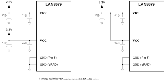
The simplest power architecture applies when the LAN8679 interfaces to a digital PHY controller using 3.3V logic and does not require a low power sleep state with wake‑up. In this architecture, both the VIO and VCC pins are connected to a common 3.3V power supply. The VCC pin supplies power to the transceiver analog and core circuitry, while the VIO pin supplies power to the digital I/O pins (TX, RX, and ED). For architectures interfacing to a digital PHY controller using 2.5V logic, the VIO pin must instead be connected to a separate 2.5V supply, while the VCC pin remains connected to a 3.3V supply. See Figure 6-1.
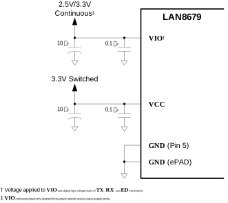
In systems implementing a low power sleep state, the VIO pin also supplies power to the internal wake detection circuitry. In this architecture, the VIO pin must be connected to a continuous, uninterrupted 3.3V or 2.5V supply, depending on the desired digital I/O pin logic; this supply must remain active even while the device is in the LOW_POWER (sleep) state. The VCC pin must be connected to a 3.3V supply that is switched off during the LOW_POWER (sleep) state to achieve minimal power consumption. See Figure 6-2.
Proper decoupling of the LAN8679 power distribution network is a prerequisite for stable operation and best EMC performance. A low ESR 0.1 μF decoupling capacitor are placed at each power pin of the device for localized decoupling. These decoupling capacitors should be located as close as possible to the respective pin to minimize parasitic inductance and maximize their effectiveness. This is typically done by placing the decoupling capacitor on the opposite side of the board from the device directly under the pin and connecting it to the exposed ground pad of the device through vias. Each decoupling capacitor is ideally connected to the power plane through two vias to minimize interconnection inductance. Decoupling capacitors should not share vias.
In addition to the decoupling capacitor at each pin, a bulk capacitor, typically 10 μF, is placed near the LAN8679 in the direction of the power supply that will be supplying current. The bulk capacitors serve to provide low frequency energy that is outside the supply’s response time.
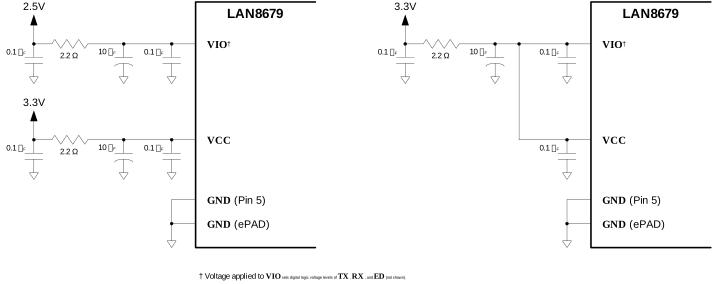
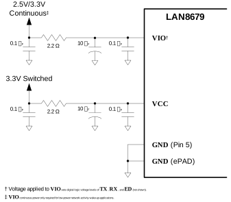
EMI sensitive applications requiring increased noise performance may optionally add a low ESR 0.1 μF capacitor and series 2.2Ω resistor to the VIO and VCC supplies as illustrated in Figure 6-3 and Figure 6-4. The combination of the capacitor and series resistance forms a low-pass filter that rejects switching noise from the device from coupling onto the circuit board power network. The 10 μF bulk capacitor must remain on the pin side of the resistor to avoid limiting its effectiveness to provide low-frequency current to the device. During the prototype phase, it is recommended to include the option for adding these components should the need arise to improve noise immunity.
Ideally, the board stackup will contain a large power plane layer next to a ground plane layer. The capacitance between the power and ground planes serves to provide high frequency, low inductance decoupling. The use of power tracks is discouraged but, if used, should be as short and wide as possible to minimize sheet resistance and current dependent voltage ripple at the power distribution to the pins.
The exposed ground pad (ePAD) of the package serves as a ground connection of the device and must be adequately connected to the PCB ground plane through an array of vias as specified in the Packaging Information section.