
4.1 AVR128DA48 Bootloader Example
Basic bootloader example using the UART driver interface with both XC8 and GCC compiler
steps.
Description: This section details a full standard bootloader use case on the AVR128DA48 microcontroller. This example applies to many variants of the AVRDA family and may also be extrapolated to other 8-bit AVR chips as well. This example uses the AVR128DA48 Curiosity Nano board purchased from Microchip. Refer to the device schematics for configuration information.
Example: This example shows how to bootload a program that blinks the LED of the AVRDA family of chips.
-
Click the New Project button in the top left of the menu.
Figure 4-1. AVR128DA48 New Project 
-
Select Standalone Project and click Next.
Figure 4-2. Choose Project Type 
-
An AVR128DA48 is used for this example. Type the name of the device into the “Device” field and MPLAB X IDE will display the options.
Figure 4-3. Select Device 
-
Select a tool for programming. The AVR128DA48 Curiosity Nano board will be used for this example as well. Select the tool from the drop-down menu and then click Next.
Note: If only ‘Simulator’ is displayed, then the target board is not plugged into the computer or it is not communicating with MPLAB X IDE properly.Figure 4-4. Select Tool 
-
In this example, the XC8 compiler v2.40 is used. However, a GCC compiler can also be used. To do this, select a GCC compiler version from the AVR-GCC drop-down menu. Click Next after selecting the compiler.
Figure 4-5. Select Compiler 
-
Type the desired project name into the Project Name field and click Next. Give it a descriptive name so the project can be easily identified.
Figure 4-6. Select Project Name and Folder 
-
Click the MCC button in the menu bar to start the Code Configurator.
Figure 4-7. Open MCC 
-
Click the Select MCC Melody button for this example.
Figure 4-8. Select MCC Melody 
-
Use the Optional Content tab to install optional libraries, such as the bootloader. If no other libraries need to be installed, click Finish.
Figure 4-9. Optional Content Tab 
-
In the previous versions of MCC, a user needed to manually attach all the peripheral drivers required by their library, using the Device Resources tab. The new MCC Melody allows users to select the library needed for the project and Melody brings in all the dependencies and configures them.
Figure 4-10. Device Resources Tab 
-
Confirm that the bootloader module has been included into the Builder window. Builder UI reflects all the required peripheral driver dependencies such as the Non-Volatile Memory (NVM), UART and Delay modules, and links them to the Bootloader library.
Figure 4-11. Builder Window 
-
One of the modules that cannot be configured automatically is the communication driver. For the bootloader to communicate with the Bootloader Host Application, a communication driver needs to be exposed to push data through the serial ports on the target device. To understand which communication ports are required to be opened for the device in use, check the schematics and look for the Serial or CDC Ports definition for the device, as shown in the image below. Using this definition, the MCU is communicating through port PC0 for transmitting data serially and port PC1 for receiving data serially.
Figure 4-12. Serial/ CDC Port for AVR128DA48 
A communication driver version that communicates through the PC0 and PC1 ports is needed. For workflows on the AVR128DA48 Curiosity Nano, attach the USART1 driver as that is the UART driver that can communicate through those ports. Select USART1 from the ‘UART PLIB Selector’ in the UART(None) tab. The USART1 settings will open up.
Figure 4-13. UART PLIB Selector  Note: Some devices will automatically select the required UART pins. Open the Pin Grid View tab to make sure the pins are enabled.
Figure 4-14. AVR128DA48 Pin Grid View 
-
Configuring the I/O pins for a bootloader has several advantages, but the most important one is receiving a state back from the MCU based on the LED. For example, the bootloader module will light up the LED when in a Boot state and it will turn off when the application state takes over. The program flow is now tracked during the development process. Telling the Bootloader module to utilize the I/O Indicator pin sets up the functionality. This is done by enabling the switch that activates the I/O Pin Indicator. For this use case, the I/O Entry Pin will also be configured. This pin is used to force the MCU into a Bootloader state by checking for voltage levels on the entry pin at any device Reset. To activate this pin, enable the UI switch from the Bootloader8-bit tab.
Figure 4-15. Options - Bootloader8-bit Tab 
-
Check the schematics to configure the I/O pin for using the LED on the board. Find the I/O interface declaration, similar to the image below. For the AVR128DA48, make sure the PC6 port is connected to control the LED.
Figure 4-16. On-Board Peripherals 
-
Go back to MPLAB X IDE and navigate to the Pin Grid View in the bottom center of the screen.
Figure 4-17. Pin Grid View Tab 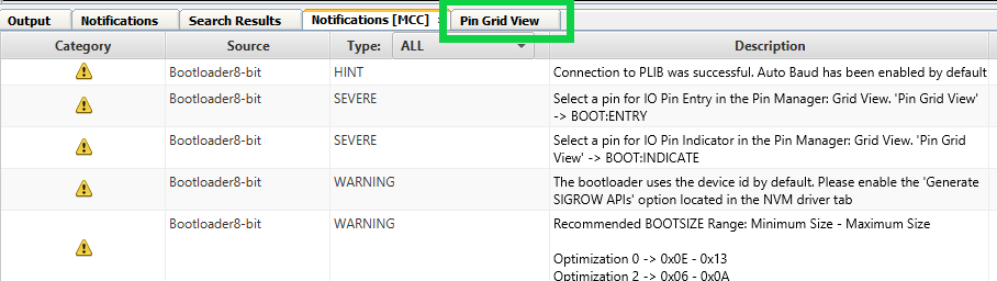
-
Select the PC6 pin for the BOOT INDICATE in the pin grid and PC7 for the BOOT ENTRY pin.
Figure 4-18. Boot Indicator and Boot Entry Pins  Note: For further configuration, access the Pins Module UI through Project Resources>System>Pins.
 -
The bootloader supports the configuration process. Address all the notifications shown in the Notifications tab. For example, “NVM options must be enabled”. Addressing the notification will either turn it into a hint or remove it from the list.
Figure 4-19. Notifications Tab 
Figure 4-20. Notifications Tab NVM Cleared 
-
Click the Generate button in the Project Resources tab to generate the initial code.
Note: This step will generate a warning on the screen. Continue the setup process.Figure 4-21. AVR128DA48 Generate Code 
-
Identify how much memory the generated code uses before configuring the bootloader memory block. To do that, use MPLAB X IDE to program the bootloader onto the target device. MPLAB X IDE displays a log after the initial programming. The log shows the memory addresses occupied by the bootloader program. Configure the bootloader’s FUSE values based on the log. Click Clean and Build and then Program Device.
Figure 4-22. Build and Program Device with Main Project 
-
With the device programmed, the next step is to calculate the FUSE size. As seen in the image above, the bootloader code is taking up memory from 0x0 to 0x6ff. The Boot section of memory needs to be configured at a minimum 0x700 in size to fit the bootloader code. The range must be pushed slightly higher to account for the RAM needed during operation. In this example, extra space is added to the bootloader to mimic a production design choice suitable for several solutions. There can also be a design where extra space is added to the Boot section to house an internal library within the Boot section of Flash.
Note: Adding extra space in the Boot section of Flash is a design decision that must be considered on an as needed basis.8-bit AVR devices utilize the FUSE settings to partition the device memory into various sections needed to support bootloading operations. Below is the configuration description for configuring the FUSE settings to reflect user needs. A bootloader requires at least two of the three sections of memory (BOOT and APPCODE) and therefore users must set a non-zero value for the Boot bit in every bootloader they implement. The Code bit can be configured if needed, but it is not required.
Note: An omitted fuse byte will be set to 0x00 and will most likely cause an unpredicted configuration.Figure 4-23. Flash Partition 
The memory range needed for the bootloader (0x700) and the extra space added (0xA00) takes the Boot space to a total memory size of 0x1000. Plug the 0x1000 into the equation mentioned below.
Note: A programming calculator must be used not a standard one, considering this equation uses hexadecimal not decimal numbers.The Boot Fuse value is now 0x08.
-
The Fuse values can be configured in two ways for the bootloader operation. The first method is to configure the size of the Boot section of memory and then allow the compiler to handle everything. For example, select a Boot fuse value of 0x08 and a Code fuse value of 0x00, resulting in a Boot section from address 0x0000 to 0x0FFF of memory, and the App section will be the rest of memory.
Note: Remember that the Boot section of Flash cannot be overwritten by the sections below it.The second method gives users more control over the various portions of memory. Set a Boot section size and an AppCode size which will automatically create a third section called AppData. For example, select a Boot fuse value of 0x08 and a Code fuse of 0x09. This results in a Boot section from address 0x0000 to 0x0FFF, the AppCode section will go from address 0x1000 to 0x11FF and the AppData will take up the rest of Flash. Use the chart below as a reference when designing device fuse settings.
Figure 4-24. Setting up Flash Sections 
-
Now set the FUSE values in Bootloader. Take the the Bootsize Fuse calculated in the last step and plug it into the Fuse UI field within the Configuration Bits tab. Click the Configuration Bits module in the Project Resources tab. Then input the value calculated into the respective field.
Figure 4-25. Configuration Bits Tab  Note: The “BOOTSIZE” field in the Configuration Bit Setup uses decimal values. Make sure to convert the calculated hex value to decimal value.
Figure 4-26. Setting the BOOTSIZE Fuse 
-
Setting the CODESIZE fuse is an optional action that can be done in instances where a user wants more control over the various portions of memory. If this value is set to 0x00, the bootloader will still operate normally but it is not possible to specify an AppData section of memory without first configuring the Codesize fuse. Refer to the memory map presented in the Fuse portion of this document for more information on how to configure this option.
Note: The “CODESIZE” field in the Configuration Bit Setup uses decimal values. Make sure to convert the calculated hex value to decimal value.Figure 4-27. Setting the CODESIZE Fuse 
-
The new code files can now be generated for the bootloader once more. After generation is complete, click the “Clean and Build” icon drop-down option and select Clean and Build Main Project to compile the bootloader code.
Figure 4-28. Generate Code and Build Main Project 
-
To prepare the chip to bootload, click the Make and Program Device button. After this programming process ends, the LED on the AVR128DA48 will illuminate and stay lit up.
Figure 4-29. Make and Program Device 
Blinking LED End Application Project
Now that the bootloader code is built and configured to specifications, configure the target application to work alongside the bootloader instead of erasing the bootloader code from the device and programming the new target application over it. MPLAB X IDE allows this by setting various project configuration properties to match the bootloader’s configuration. The first step for completing this task is to create a Blinking LED Project.
-
Create another new Standalone project, name it something notable and set it as the main project in MPLAB X IDE.
Figure 4-30. AVR128DA48 Blinking LED Application Project 
-
One important part of the development process to follow is the idea of creating multiple configurations for the target application. This allows users to create various application images that can be used for different purposes at the same time, and the bootloader uses this concept extensively.
This example needs two configurations: default and offset. The offset configuration is needed to program the bootloader and the end application onto the same chip. Start by navigating up to the configuration drop-down menu and click Customize.
Figure 4-31. Custom Configurations 
-
Click the Manage Configurations button at the bottom left of the Project Properties window.
Go to Duplicate to duplicate the default configuration, then select Rename and type in “Offset”. Click Ok.
Figure 4-32. Manage Configurations (Project Properties) 
Figure 4-33. Duplicate Configuration 
Figure 4-34. Rename Duplicated Configuration 
-
Set the offset configuration as the active configuration for the project. Click the Set Active button while the offset configuration is highlighted in blue. Once Offset has been set as the active configuration, close this window.
Figure 4-35. Set Active New Configuration 
-
Open MCC to configure the LED for the blinking light application. Click the “MCC” icon in the menu bar to start the MPLAB Code Configurator.
Figure 4-36. Open MCC 
-
Set PC6 as the LED pin and provide a custom name for the LED. Click the Generate code to generate the project code.
Figure 4-37. LED Pin 
-
The delay timer can be found in Device Resources: Drivers>Timer>Delay.
Figure 4-38. Delay Driver 
-
Generate the code using the Generate button in Project Resources. Then open the
main.cfile and add the following logic:#include "mcc_generated_files/system/system.h" #include "mcc_generated_files/timer/delay.h" /* Main application */ int main(void) { SYSTEM_Initialize(); while(1) { DELAY_milliseconds(500); LED0_Toggle(); } } -
These next steps are dependent on the compiler used in MPLAB X IDE and will change slightly due to that. For both XC8 and GCC compilers, specify where the text memory range of the end application starts. This setting is required for the compiler to program the end application into the correct range of memory and prevent overwriting the bootloader code.
-
XC8
Navigate to the Project Properties>XC8 Linker.
Figure 4-39. Project Properties - Offset Configuration 
Then, navigate to Additional Options using the drop-down menu.
Figure 4-40. Project Properties - Additional Options 
In the Extra Linker Options text box, double click and type the following options:
-Wl, -Ttext=0x1000Click OK when finished.
Note: For XC8, the 0x1000 in this linker option was taken directly from the bootloader Fuse configuration. The length of the Boot Space is passed so the linker knows where to write the end application code.Figure 4-41. Additional Options - Extra Linker Options - XC8 
-
AVR GCC
There is a slight difference in steps to be followed between the GCC compiler and the XC8 compiler. The process starts the same: navigate to Project Properties>avr-ld, Then select Memory Settings from the drop down.
Then simply use the mathematics described for setting the text range in XC8, but using the GCC linker option format. For GCC type the following line into the FLASH segment text box.
Note: This value is in words. Therefore, divide the value set in the bootloader (0x1000) by 0x2 to get this value of 0x800..text=0x800Figure 4-42. Additional Options - Extra Linker Options - GCC 
-
-
Click Clean and Build to set the offset configuration for the blinking light application. This is the application image used for bootloading.
Figure 4-43. Clean and Build Main Project 
Opening and Configuring the Unified Bootloader Host Application (UBHA)
-
Launch Unified Bootloader Host application and select File>Open/Load File. Make sure to open the
<application-MPLABX-project/dist/Offset/production/application Hex file>.Figure 4-44. UBHA - Open/Load File 
-
Next, select the type of architecture. Choose AVR128D family for this example.
Figure 4-45. UBHA Device Architecture 
-
Configure the COM port number to pass the command strings from the UBHA to the bootloader. Select Settings>Serial and then configure the COM port from the given options. To find the COM port in Windows, hit the Windows key and type “Device Manager”. Once the device manager has started, open the Ports tab and look for Virtual COM Port. That port will be used to bootload an application with the UBHA.
Figure 4-46. Device Manager - COM Port Number 
Figure 4-47. UBHA Settings - Serial 
Figure 4-48. UBHA Serial Port Settings 
-
Before beginning the programming process with the UBHA, open the Console of the app where the logs that are returned from the bootloader will be displayed. Click Tools>Console and the Program Device button to begin the bootloading process.
Figure 4-49. UBHA Console Window 
Figure 4-50. UBHA Program Device 
AVR Post Build Steps
-
Utilizing a post build step makes it possible to perform analysis and prep the application image in ways that a normal compiler cannot. This section discusses how to configure a post build script for AVR applications and how to create the CRC32 verification ready image from the blinking light application. Refer to the CRC Verification Scheme section for more information.
-
Start by creating a new file in the blinking light application folder by opening the Files tab. Right click the project folder and select New>Other.
Figure 4-51. Create New File 
-
Select Shell Scripts>Bourne Shell Script (
.sh).Figure 4-52. Shell Script - Bourne Shell Script 
-
Name the new script and click Finish.
Figure 4-53. Name New Shell Script 
-
-
Many things can be done using Hexmate with the application image. This example explains a general post build script for the bootloader applications that can be used to prepare an application for any of the hashed verification schemes supported. User can also use this script as a reference to write a new Hexmate script in the future. Copy the script here into the newly created
.shscript file and save it.Note:This script is developed using a BOOT FUSE value of 0x08.
E.g., 0x08 * 0x200 = 0x1000.
REM Fill Unimplemented Flash Space with 0xFF hexmate r0-FFFFFFFF,%2 -O%2 -FILL=w1:0xFF@0x1000:0x1FFFF if %1 == CRC16 REM Calculate CRC-16 and store at footer if %1 == CRC16 hexmate %2 -O%2 +-CK=1000-1FFFD@1FFFE+FFFFg5w-2p1021 if %1 == CRC32 REM Calculate CRC-32 and store at footer if %1 == CRC32 hexmate %2 -O%2 +-CK=1000-1FFFB@1FFFC+FFFFFFFFg-5w-4p04C11DB7 if %1 == CHECKSUM REM Calculate Checksum and store at footer if %1 == CHECKSUM hexmate %2 -O%2 +-CK=1000-1FFFD@1FFFEg2w-2 -
For Windows, create this exact same script but as a
.batfile instead. To do this, right click and copy. Then right clickAVR128DA48_Appand paste a new copy of the script file.Figure 4-54. Post Build Script for Windows 
Right click the new copy of the script and select Properties.
Figure 4-55. Properties - Shell Script 
Rename the file back to the original name from the copy and then set the extension to bat.
Figure 4-56. postBuildStep.bat - Properties 
-
The last step to configuring the post build script is to create a new project configuration that can run the script with the required inputs for Hexmate. Open the project properties of the application project and create a copy of the Offset configuration. Rename it to CRC32 and then populate the Building settings with:
postBuildStep${ShExtension} CRC32 ${ImagePath}Note: To utilize this script for any of the verification schemes, replace CRC32 with either CRC16 or CHECKSUM in the command seen above.Figure 4-57. Add Post Build Script Execution 
-
Click Clean and Build in the application. Hexmate commands can be seen running in the output window after the initial compilation succeeded.
Figure 4-58. Clean and Build with Post Build Script 
See how the last spaces in the image file are filled with data, by opening the CRC32 configuration hex file.
Figure 4-59. Generated Hex File 