The Security register supports byte writes, page writes and partial page writes in the upper 16 bytes of the region. Page writes and partial page writes in the Security register have the same page boundary restrictions and behavior as they do in the EEPROM region (see Page Write).
Writing in the Security register requires beginning the device address byte with
1011b (Bh), matching the hardware address bits (A2, A1) to the
corresponding value determined by the ordering code of the device (see Table 3 and Table 4) and sending a logic ‘0’ in the Read/Write Select
bit. The device will ACK this sequence.
Following the device address byte, bits A7 and A6 of the word address byte must be set to
10b regardless of the intended address being written. Refer to
Table 5 for detailed requirements on these bits. Figure 1 is an example of a byte write operation in
the Security register.
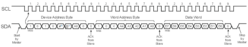
- 1. For the AT24CSW04X, the @ indicates the A1 address bit which is managed by the ordering code of the device (see Table 3). For the AT24CSW08X, the @ indicates the A9 address bit.
- 2. # indicates the hardware address value which is managed by the ordering code of the device (see Table 3 and Table 4).
The user-programmable portion of the Security register can be permanently inhibited from future writing with the Lock command. The status of the Lock state can be determined by sending a subset of the Lock command.