The conversion clock source is selected with
the CS bit. When CS = 1, the ADC clock source is an
internal fixed-frequency clock referred to as ADCRC. When CS = 0, the
ADC clock source is derived from FOSC.
Important: When CS =
0, the clock can be divided using the ADCLK register
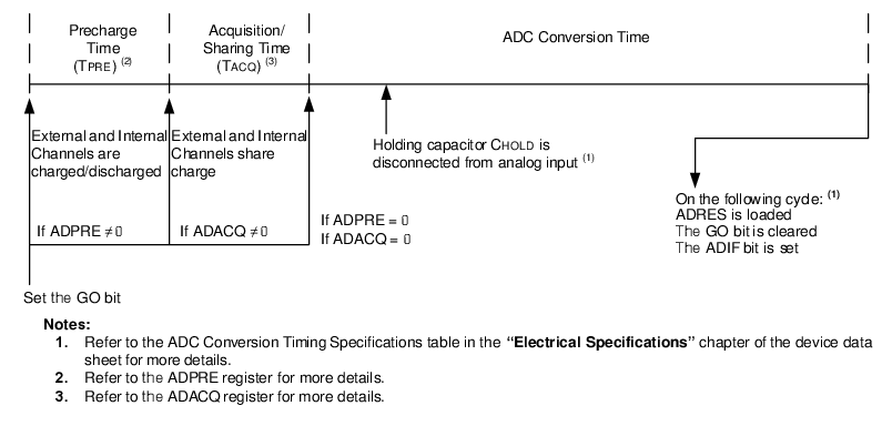
to meet the ADC clock period requirements.The time to complete one bit conversion is defined as the TAD. Refer to Figure 1 for the complete timing details of the ADC conversion.
For correct conversion, the appropriate TAD specification must be met. Refer to the ADC Timing Specifications table in the “Electrical Specifications” chapter of the device data sheet for more details. The table below gives examples of appropriate ADC clock selections.
| ADC Clock Source | ADCLK | ADC Clock Period (TAD) for Different Device Frequency (FOSC) | |||||
|---|---|---|---|---|---|---|---|
| 32 MHz | 20 MHz | 16 MHz | 8 MHz | 4 MHz | 1 MHz | ||
| FOSC/2 | ‘b000000 |
62.5 ns(2) | 100 ns(2) | 125 ns(2) | 250 ns(2) | 500 ns | 2.0 μs |
| FOSC/4 | ‘b000001 |
125 ns(2) | 200 ns(2) | 250 ns(2) | 500 ns | 1.0 μs | 4.0 μs |
| FOSC/6 | ‘b000010 |
187.5 ns(2) | 300 ns(2) | 375 ns(2) | 750 ns | 1.5 μs | 6.0 μs |
| FOSC/8 | ‘b000011 |
250 ns(2) | 400 ns(2) | 500 ns | 1.0 μs | 2.0 μs | 8.0 μs |
| ... | ... | ... | ... | ... | ... | ... | ... |
| FOSC/16 | ‘b000111 |
500 ns | 800 ns | 1.0 μs | 2.0 μs | 4.0 μs | 16.0 μs(2) |
| ... | ... | ... | ... | ... | ... | ... | ... |
| FOSC/32 | ‘b001111 |
1.0 μs | 1.6 μs | 2.0 μs | 4.0 μs | 8.0 μs | 32.0 μs(2) |
| ... | ... | ... | ... | ... | ... | ... | ... |
| FOSC/64 | ‘b0111111 |
2.0 μs | 3.2 μs | 4.0 μs | 8.0 μs | 16.0 μs(2) | 64.0 μs(2) |
| ... | ... | ... | ... | ... | ... | ... | ... |
| FOSC/128 | ‘b111111 |
4.0 μs | 6.4 μs | 8.0 μs | 16.0 μs(2) | 32.0 μs(2) | 128.0 μs(2) |
| ADCRC | CS = 1 |
1.0-6.0 μs | 1.0-6.0 μs | 1.0-6.0 μs | 1.0-6.0 μs | 1.0-6.0 μs | 1.0-6.0 μs |
|
Notes:
|
|||||||
Important:
- Except for the ADCRC clock source, any changes in the system clock frequency will change the ADC clock frequency, which may adversely affect the ADC result.
- The internal control logic of the
ADC runs off of the clock selected by the CS bit. When the CS bit is set to
‘
1’ (ADC runs on ADCRC), there may be unexpected delays in operation when setting the ADC control bits.
Figure 1. Analog-to-Digital Conversion Cycles