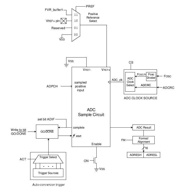
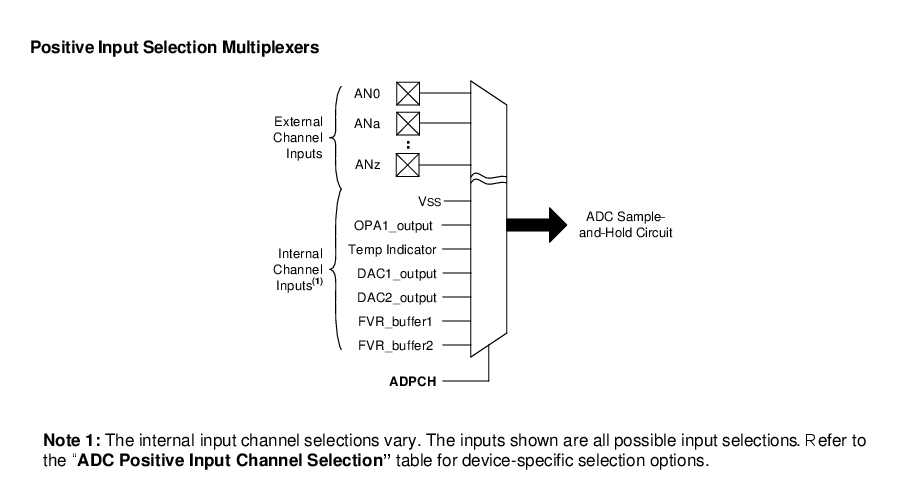
The Analog-to-Digital Converter with Computation module allows conversion of single-ended analog input signals to a 10-bit binary representation of that signal. This device uses analog inputs that are multiplexed into a single Sample-and-Hold circuit. The output of the Sample-and-Hold (S/H) circuit is connected to the input of the converter. The converter generates a 10-bit binary result via successive approximation and stores the conversion result into the ADC result registers. In single-ended conversions, the ADC measures the voltage between the selected analog input and VSS (0V). The selected ADC input channels can either be from an internal source, such as the Fixed Voltage Reference (FVR), or from external analog input pins. Additionally, the following features are provided within the ADC module:
- Acquisition Timer
- Hardware Capacitive Voltage Divider (CVD)
support:
- Precharge timer
- Adjustable Sample-and-Hold capacitor array
- Guard ring digital output drive
- Automatic Repeat and Sequencing:
- Automated double sample conversion for CVD
- Two sets of Result registers (Current Result and Previous Result)
- Auto-conversion trigger
- Internal retrigger
- Channel Grouping:
- Allows multiple input channels to be grouped together into a single input channel
- Computation Features:
- Averaging and low-pass filter functions
- Reference comparison
- 2-level threshold comparison
- Selectable interrupts
Figure 43-1 shows the block diagram of the ADC.
The ADC positive voltage reference is software selectable to be either internally generated or externally supplied. The ADC negative voltage reference is internally connected to VSS.
The ADC can generate an interrupt upon completion of a conversion and upon threshold comparison. These interrupts can be used to wake up the device from Sleep.